CET4435A
CET4435A is P-Channel MOSFET manufactured by Chino-Excel Technology.
- Part of the CET4435A_Chino comparator family.
- Part of the CET4435A_Chino comparator family.
P-Channel Enhancement Mode Field Effect Transistor Features
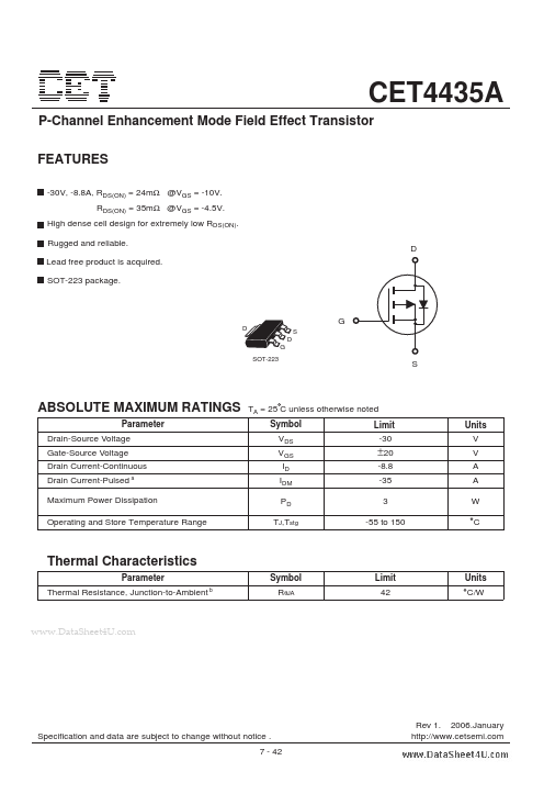
-30V, -8.8A, RDS(ON) = 24mΩ @VGS = -10V. RDS(ON) = 35mΩ @VGS = -4.5V. High dense cell design for extremely low RDS(ON). Rugged and reliable. Lead free product is acquired. SOT-223 package. D
D D G...