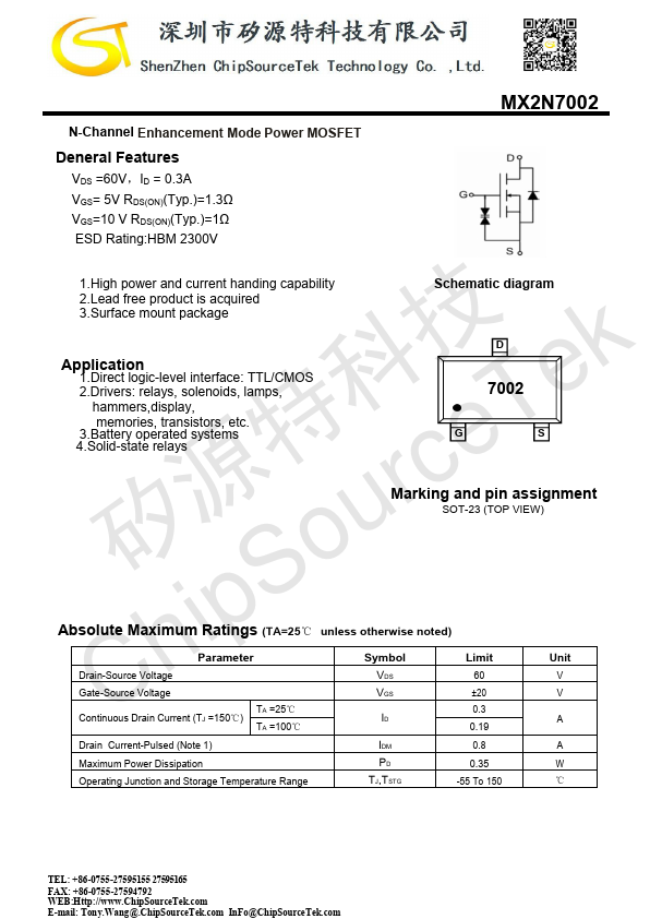
MX2N7002 Overview
N-Channel Enhancement Mode Power MOSFET Deneral.
MX2N7002 datasheet by ChipSourceTek.
| Part number | MX2N7002 |
|---|---|
| Datasheet | MX2N7002-ChipSourceTek.pdf |
| File Size | 1.44 MB |
| Manufacturer | ChipSourceTek |
| Description | N-Channel Enhancement Mode Power MOSFET |
|
|
N-Channel Enhancement Mode Power MOSFET Deneral.
View all ChipSourceTek datasheets
| Part Number | Description |
|---|---|
| MX2120 | Dual-cell lithium battery protection |
| MX2120CB | Dual-cell lithium battery protection |
| MX2210N | Single-cell lithium battery protection |
| MX2300 | N-Channel Enhancement Mode Power MOSFET |
| MX2300C | N-Channel Power MOSFET |
| MX2301 | P-Channel Power MOSFET |
| MX2301A | P-Channel Power MOSFET |
| MX2302A | N-Channel Power MOSFET |
| MX2305 | P-Channel Power MOSFET |
| MX2319 | P-Channel Enhancement Mode Power MOSFET |