Datasheet4U Logo Datasheet4U.com

CY2302 Datasheet Frequency Multiplier And Zero Delay Buffer

Manufacturer: Cypress (now Infineon)

General Description

Reference Input: The output signals are synchronized to this signal.

Feedback Input: This input must be fed by one of the outputs (OUT1 or OUT2) to ensure proper functionality.

If the trace between FBIN and the output pin being used for feedback is equal in length to the traces between the outputs and the signal destinations, then the signals received at the destinations are synchronized to the REF signal input (IN).

Key Features

  • 90 ps typical jitter OUT2.
  • 200 ps typical jitter OUT1.
  • 65 ps typical output-to-output skew.
  • 90 ps typical propagation delay.
  • Voltage range: 3.3 V±5%, or 5 V±10%.
  • Output frequency range: 5 MHz to 133 MHz.
  • Two outputs.
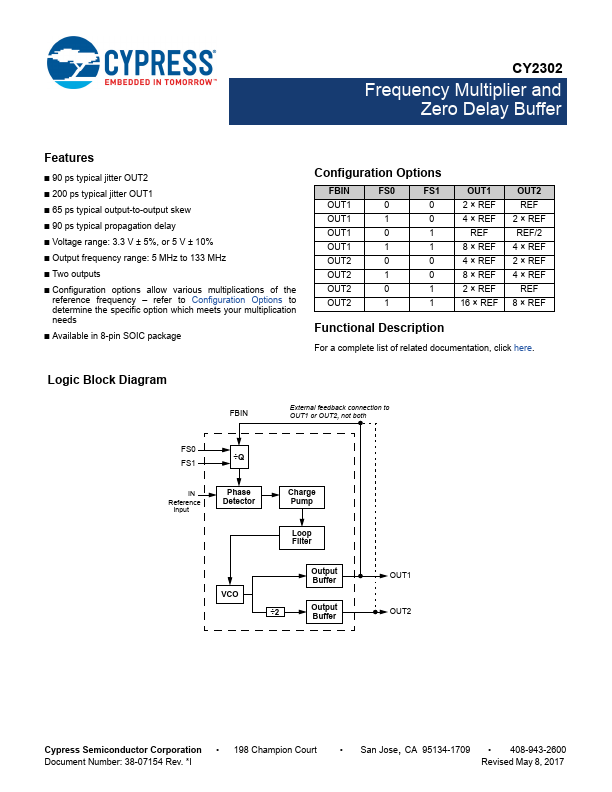
  • Configuration options allow various multiplications of the reference frequency.
  • refer to Table 1 to determine the specific option which meets your multiplication needs.
  • Available in 8-pin SOIC package CY2302 Frequency Multiplier.

CY2302 Distributor