CY2308
Overview
- Zero input-output propagation delay, adjustable by capacitive load on FBK input
- Multiple configurations, see Available CY2308 Configurations on page 4 for more details
- Multiple low skew outputs
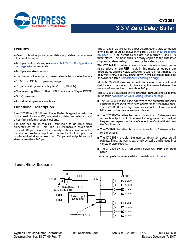
- Two banks of four outputs, three-stateable by two select inputs
- 10 MHz to 133 MHz operating range
- 75 ps typical cycle-to-cycle jitter (15 pF, 66 MHz)
- Space saving 16-pin 150 mil SOIC package or 16-pin TSSOP
- 3.3 V operation
- Industrial temperature available Functional Description The CY2308 is a 3.3 V Zero Delay Buffer designed to distribute high speed clocks in PC, workstation, datacom, telecom, and other high performance applications. The part has an on-chip PLL that locks to an input clock presented on the REF pin. The PLL feedback is driven from external FBK pin, so user has flexibility to choose any one of the outputs as feedback input and connect it to FBK pin. The input-to-output skew is les