CY2304
Overview
- Zero input-output propagation delay, adjustable by capacitive load on FBK input
- Multiple configurations
- Multiple low-skew outputs
- 10 MHz to 133 MHz operating range
- 90 ps typical peak cycle-to-cycle jitter at 15 pF, 66 MHz
- Space-saving 8-pin 150-mil small outline integrated circuit (SOIC) package
- 3.3 V operation
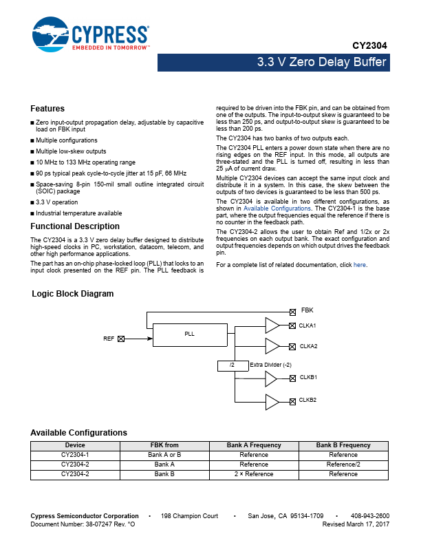
- Industrial temperature available Functional Description The CY2304 is a 3.3 V zero delay buffer designed to distribute high-speed clocks in PC, workstation, datacom, telecom, and other high performance applications. The part has an on-chip phase-locked loop (PLL) that locks to an input clock presented on the REF pin. The PLL feedback is required to be driven into the FBK pin, and can be obtained from one of the outputs. The input-to-output skew is guaranteed to be less than 250 ps, and output-to-output skew is guaranteed to be less than 200 ps. The CY2304 has two banks of two output