CY27410
CY27410 is 4-PLL Spread-Spectrum Clock Generator manufactured by Cypress.
4-PLL Spread-Spectrum Clock Generator
4-PLL Spread-Spectrum Clock Generator
Features
- Input frequencies
- Crystal input: 8 MHz to 48 MHz
- Reference clock: 8 MHz to 250 MHz LVCMOS
- Reference clock: 8 MHz to 700 MHz differential
- Output frequencies
- 25 MHz to 700 MHz LVDS, LVPECL, HCSL, CML
- 3 MHz to 250 MHz LVCMOS
- 1 k Hz to 8 MHz for one LVCMOS output
- RMS phase jitter: 1-ps max at 12-k Hz to 20-MHz offset
- PCIe 1.0/2.0/3.0 pliant
- SATA 2.0, USB 2.0/3.0, 1/10-Gb E pliant
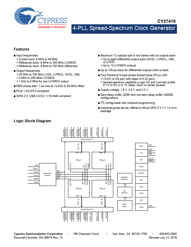
Logic Block Diagram
- Maximum 12 outputs split in two banks with six outputs each.
- Up to eight differential output pairs (HCSL, LVPECL, CML, or LVDS)
- Up to 12 LVCMOS outputs
- Up to 100-ps skew for differential outputs within a bank
- Four fractional N-type phase-locked loops (PLLs) with
- VCXO (±120 ppm with steps of 0.23 ppm)
- Spread-spectrum capability (Logic SS and Lexmark profile 0.1% to 5% in 0.1% steps, down or center spread)
- Supply voltage:...