CY27EE16ZE
CY27EE16ZE is 1 PLL In-System Programmable Clock Generator with Individual 16K EEPROM manufactured by Cypress.
1 PLL In-System Programmable Clock Generator with Individual 16K EEPROM
Features
- 18 kbits of EEPROM 16 kbits independent scratch 2 kbits dedicated to clocking functions Benefits Higher level of integration and reduced ponent count by bining EEPROM and PLL. Independent EEPROM may be used for scratch memory, or to store up to eight clock configurations
- Integrated, phase-locked loop with programmable P High-performance PLL enables control of output frequencies that are and Q counters, output dividers, and optional customizable to support a wide range of applications analog VCXO, digital VCXO, spread spectrum for EMI reduction
- In system programmable through I2C Serial Programming Interface (SPI). Both the SRAM and non-volatile EEPROM memory bits are programmable with the 3.3V supply
- Low-jitter, high-accuracy outputs
- VCXO with analog adjust Familiar industry standard eases programming effort and enables update of data stored in 16K EEPROM scratchpad and 2K EEPROM clock control block while CY27EE16ZE is installed in system Meets critical timing requirements in plex system designs Write Protect (WP pin) can be programmed to serve as an analog control voltage for a VCXO.The VCXO function is still available with a DCXO, or digitally controlled (through SPI) crystal oscillator if the pin is functioning as WP Meets industry-standard voltage platforms Industry standard packaging saves on board space Input Frequency Range Output Frequency Range
- 3.3V Operation (optional 2.5V outputs)
- 20-lead Exposed Pad, EP-TSSOP Part Number CY27EE16ZE Outputs 6
- 167 MHz (Driven Clock Input) {mercial} 80 k Hz
- 200 MHz (3.3V) {mercial} 1
- 150 MHz (Driven Clock Input) {Industrial} 80 k Hz
- 167 MHz (3.3V) {Industrial} 8
- 30 MHz (Crystal Reference) {m. or Ind.} 80 k Hz
- 167 MHz (2.5V) {mercial} 80 k Hz
- 150 MHz (2.5V) {Industrial}
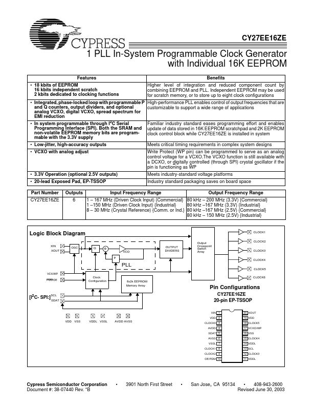
Logic Block Diagram
XIN XOUT OSC Q Φ VCO P OUTPUT DIVIDERS Output Crosspoint Switch Array
CLOCK1
CLOCK2
CLOCK3
CLOC...