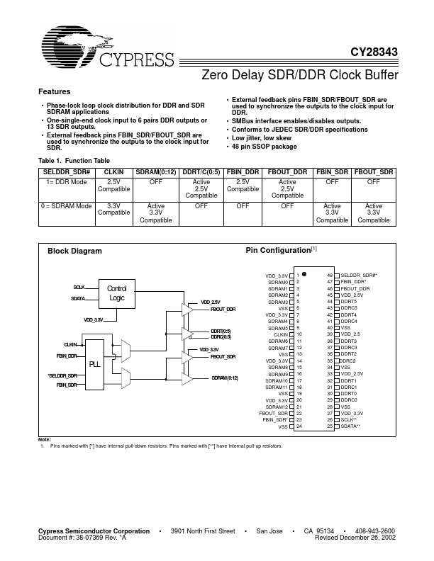
Datasheet4U Logo Datasheet4U.com

CY28343 - Zero Delay SDR/DDR Clock Buffer

General Description

Pin 10 47 23 30,32,36,38 42,44 29,31,35,37 41,43 2-5,8,9 15-18,21 46 Name CLKIN FBIN_DDR FBIN_SDR DDRT(0:5) DDRC(0:5) SDRAM(0:12) FBOUT_DDR I/O I I PD I PD O O O O Clock Input.

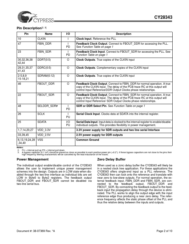
Reference the PLL Feedback Clock Output.

Connect to FBOUT_DDR for accessing the PLL.

Key Features

  • Phase-lock loop clock distribution for DDR and SDR SDRAM.

📥 Download Datasheet

Full PDF Text Transcription (Reference)

The following content is an automatically extracted verbatim text from the original manufacturer datasheet and is provided for reference purposes only.

View original datasheet text
CY28343 Zero Delay SDR/DDR Clock Buffer Features • Phase-lock loop clock distribution for DDR and SDR SDRAM applications • One-single-end clock input to 6 pairs DDR outputs or 13 SDR outputs. • External feedback pins FBIN_SDR/FBOUT_SDR are used to synchronize the outputs to the clock input for SDR. Table 1. Function Table SELDDR_SDR# 1= DDR Mode CLKIN 2.5V Compatible 3.3V Compatible SDRAM(0:12) OFF DDRT/C(0:5) Active 2.5V Compatible OFF FBIN_DDR 2.5V Compatible OFF FBOUT_DDR Active 2.5V Compatible OFF FBIN_SDR FBOUT_SDR OFF OFF • External feedback pins FBIN_SDR/FBOUT_SDR are used to synchronize the outputs to the clock input for DDR. • SMBus interface enables/disables outputs.