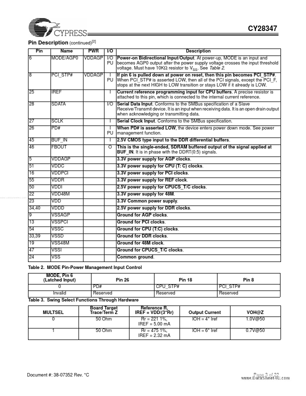
CY28347 Description
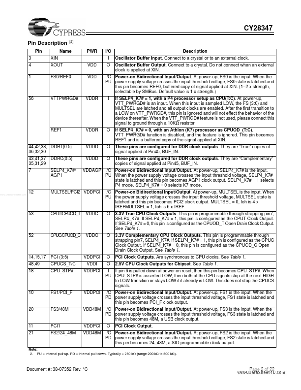
Pin 3 4 1 XIN XOUT FS0/REF0 VDD VDD [2] Name PWR I/O I O Description Oscillator Buffer Input. Connect to a crystal or to an external clock. Oscillator Buffer Output.
CY28347 Key Features
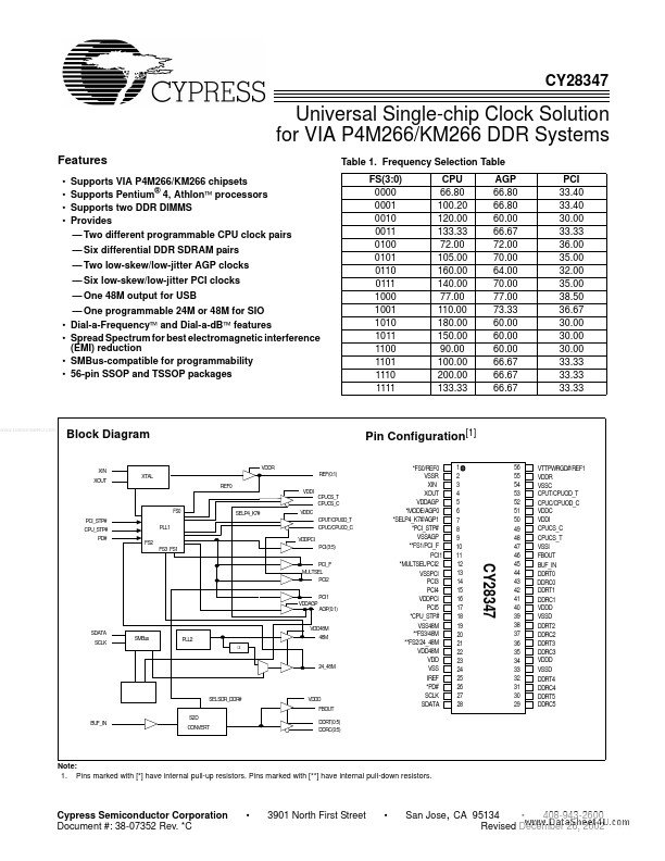
- Supports VIA P4M266/KM266 chipsets Supports Pentium® 4, Athlon processors Supports two DDR DIMMS Provides
- Two different programmable CPU clock pairs
- Six differential DDR SDRAM pairs
- Two low-skew/low-jitter AGP clocks
- Six low-skew/low-jitter PCI clocks
- One 48M output for USB
- One programmable 24M or 48M for SIO
- Dial-a-Frequency and Dial-a-dB features
- Spread Spectrum for best electromagnetic interference (EMI) reduction
- SMBus-patible for programmability