CY2PD817
CY2PD817 is PECL/CMOS Buffer manufactured by Cypress.
..
320-MHz 1:7 PECL to PECL/CMOS Buffer
Features
- -
- -
- -
- -
- -
- -
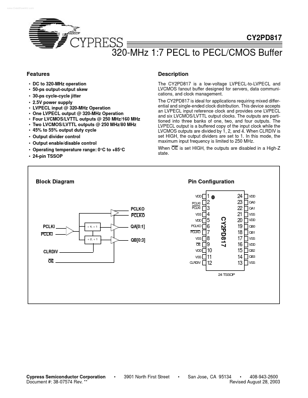
- DC to 320-MHz operation 50-ps output-output skew 30-ps cycle-cycle jitter 2.5V power supply LVPECL input @ 320-MHz Operation One LVPECL output @ 320-MHz Operation Four LVCMOS/LVTTL outputs @ 250 MHz/160 MHz Two LVCMOS/LVTTL outputs @ 250 MHz/80 MHz 45% to 55% output duty cycle Output divider control Output enable/disable control Operating temperature range: 0°C to +85°C 24-pin TSSOP
Description
The CY2PD817 is a low-voltage LVPECL-to-LVPECL and LVCMOS fanout buffer designed for servers, data munications, and clock management. The CY2PD817 is ideal for applications requiring mixed...