CY2PP326
CY2PP326 is 2 x 2 Clock and Data Switch Buffer manufactured by Cypress.
FastEdge™ Series CY2PP326
..
2 x 2 Clock and Data Switch Buffer
Features
- Six ECL/PECL differential outputs
- Two ECL/PECL differential inputs
- Hot-swappable/-insertable
- 50 ps output-to-output skew
- 250 ps device-to-device skew
- 950 ps propagation delay (typical)
- 1.2 GHz Operation
- 2.8 ps RMS period jitter (max.)
- PECL mode supply range: VEE =
- 2.5V± 5% to
- 3.3V±5% with VEE = 0V
- ECL mode supply range: VCC = 2.5V± 5% to 3.3V±5% with VEE = 0V
- Industrial temperature range:
- 40°C to 85°C
- 32-pin 1.4mm TQFP package
- Temperature pensation like 100K ECL
- Pin patible with MC100ES6254
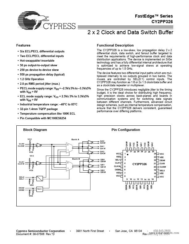
Functional Description
The CY2PP326 is a low-skew, low propagation delay...