CY7B9940V
Overview
- 12-100 MHz (CY7B9930V), or 24-200 MHz (CY7B9940V) input/output operation Matched pair output skew < 200 ps Zero input-to-output delay 10 LVTTL 50% duty-cycle outputs capable of driving 50ω terminated lines Commercial temperature range with eight outputs at 200 MHz Industrial temperature range with eight outputs at 200 MHz 3.3V LVTTL/LV differential (LVPECL), fault-tolerant and hot insertable reference inputs Multiply ratios of (1-6, 8, 10, 12) Operation up to 12x input frequency Individual output bank disable for aggressive power management and EMI reduction Output high impedance option for testing purposes Fully integrated PLL with lock indicator Low cycle-to-cycle jitter (<100 ps peak-peak) *
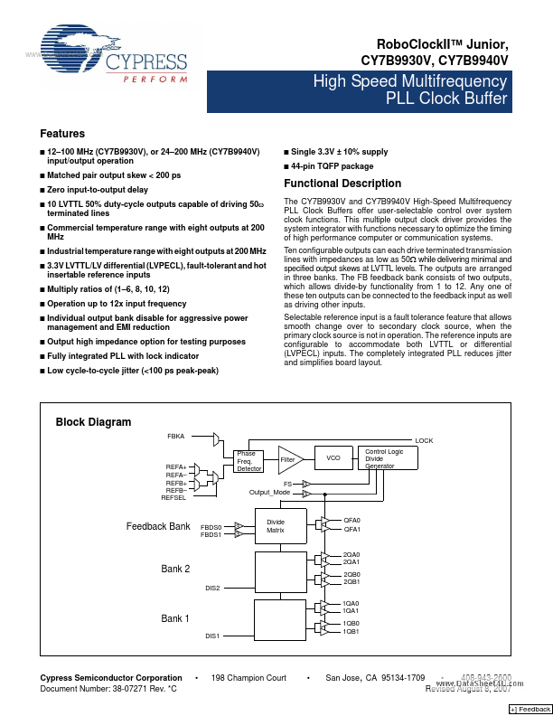
- Single 3.3V ± 10% supply 44-pin TQFP package Functional Description The CY7B9930V and CY7B9940V High-Speed Multifrequency PLL Clock Buffers offer user-selectable control over system clock functions. This multiple output clock driver provides the system integrator with functions necessary to optimize the timing of high performance computer or communication systems. Ten configurable outputs can each drive terminated transmission lines with impedances as low as 50Ω while delivering minimal and specified output skews at LVTTL levels. The outputs are arranged in three banks. The FB feedback bank consists of two outputs, which allows divide-by functionality from 1 to
- Any one of these ten outputs can be connected to the feedback input as well as driving other inputs. Selectable reference input is a fault tolerance feature that allows smooth change over to secondary clock source, when the primary clock source is not in operation. The reference inputs are configurable to accommodate both LVTTL or differential (LVPECL) inputs. The completely integrated PLL reduces jitter and simplifies board layo