CY7C1041BV33
CY7C1041BV33 is 256K x 16 Static RAM manufactured by Cypress.
- Part of the CY7 comparator family.
- Part of the CY7 comparator family.
041BV33
256K x 16 Static RAM
Features
- High speed
- t AA = 12 ns
- Low active power
- 612 m W (max.)
- Low CMOS standby power (mercial L version)
- 1.8 m W (max.)
- 2.0V Data Retention (600 µW at 2.0V retention)
- Automatic power-down when deselected
- TTL-patible inputs and outputs
- Easy memory expansion with CE and OE Features written into the location specified on the address pins (A0 through A17). If Byte High Enable (BHE) is LOW, then data from I/O pins (I/O8 through I/O15) is written into the location specified on the address pins (A0 through A17). Reading from the device is acplished by taking Chip Enable (CE) and Output Enable (OE) LOW while forcing the Write Enable (WE) HIGH. If Byte Low Enable (BLE) is LOW, then data from the memory location specified by the address pins will appear on I/O0 to I/O7. If Byte High Enable (BHE) is LOW, then data from memory will appear on I/O8 to I/O15. See the truth table at the back of this data sheet for a plete description of read and write modes. The input/output pins (I/O0 through I/O15) are placed in a high-impedance state when the device is deselected (CE HIGH), the outputs are disabled (OE HIGH), the BHE and BLE are disabled (BHE, BLE HIGH), or during a write operation (CE LOW, and WE LOW). The CY7C1041BV33 is available in a standard 44-pin 400-mil-wide body width SOJ and 44-pin TSOP II package with center power and ground (revolutionary) pinout.
Functional Description
The CY7C1041BV33 is a high-performance CMOS Static RAM organized as 262,144 words by 16 bits. Writing to the device is acplished by taking Chip Enable (CE) and Write Enable (WE) inputs LOW. If Byte Low Enable (BLE) is LOW, then data from I/O pins (I/O0 through I/O7), is
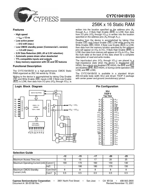
Logic Block Diagram
INPUT BUFFER
Pin Configuration
SOJ TSOP II Top View A0 A1 A2 A3 A4 CE I/O0 I/O1 I/O2 I/O3 VCC VSS I/O4 I/O5 I/O6 I/O7 WE A5 A6 A7 A8 A9
1 2 3 4 5 6 7 8 9 10 11 12 13 14 15 16 17 18 19 20 21 22 44 43 42 41 40 39 38 37 36 35 34 33 32...