CY7C1069AV33
CY7C1069AV33 is 2M x 8 Static RAM manufactured by Cypress.
- Part of the CY7 comparator family.
- Part of the CY7 comparator family.
2M x 8 Static RAM
Features
- High speed
- t AA = 8, 10, 12 ns
- Low active power
- 1080 m W (max.)
- Operating voltages of 3.3 ± 0.3V
- 2.0V data retention
- Automatic power-down when deselected
- TTL-patible inputs and outputs
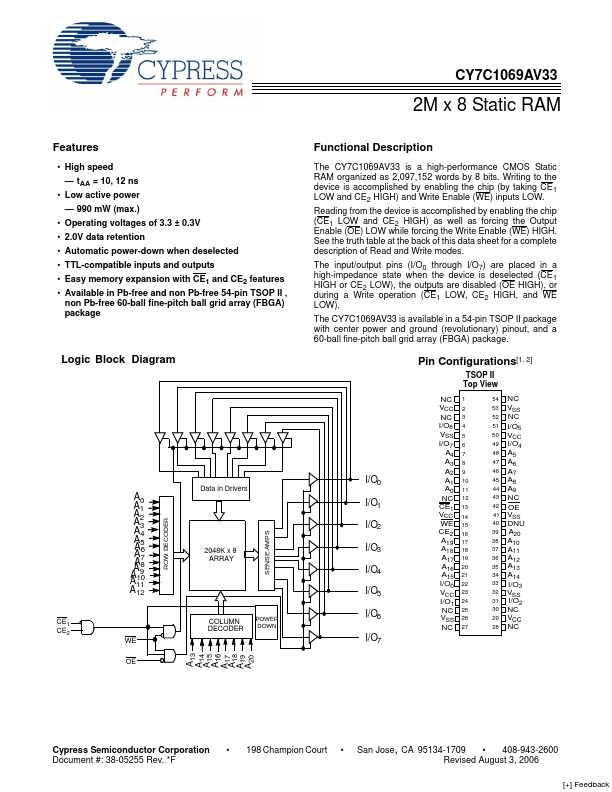
- Easy memory expansion with CE1 and CE2 Features device is acplished by enabling the chip (by taking CE1 LOW and CE2 HIGH) and Write Enable (WE) inputs LOW. Reading from the device is acplished by enabling the chip (CE1 LOW and CE2 HIGH) as well as forcing the Output Enable (OE) LOW while forcing the Write Enable (WE) HIGH. See the truth table at the back of this data sheet for a plete description of Read and Write modes. The input/output pins (I/O0 through I/O7) are placed in a high-impedance state when the device is deselected (CE1 HIGH or CE2 LOW), the outputs are disabled (OE HIGH), or during a Write operation (CE1 LOW, CE2 HIGH, and WE LOW). The CY7C1069AV33 is available in a 54-pin TSOP II package with center power and ground (revolutionary) pinout, and a 48-ball fine-pitch ball grid array (FBGA) package.
Functional Description
The CY7C1069AV33 is a high-performance CMOS Static RAM organized as 2,097,152 words by 8 bits. Writing to the
Logic Block Diagram
Pin Configuration
TSOP II Top View
INPUT BUFFER
A0 A1 A2 A3 A4 A5 A6 A7 A8 A9
2M x 8 ARRAY 4096 x 4096
I/O0- I/O7
COLUMN DECODER
WE CE2 OE CE1
NC VCC NC I/O6 VSS I/O7 A4 A3 A2 A1 A0 NC CE1 VCC WE CE2 A19 A18 A17 A16 A15 I/O0 VCC I/O1 NC VSS NC
1 2 3 4 5 6 7 8 9 10 11 12 13 14 15 16 17 18 19 20 21 22 23 24 25 26 27
54 53 52 51 50 49 48 47 46 45 44 43 42 41 40 39 38 37 36 35 34 33 32 31 30 29 28
NC VSS NC I/O5 VCC I/O4 A5 A6 A7 A8 A9 NC OE VSS DNU A20 A10 A11 A12 A13 A14 I/O3 VSS I/O2 NC
ROW DECODER
A10 A11 A 12 A 13 A 14 A15 A16 A17 A18 A19 A20
SENSE AMPS
Selection...