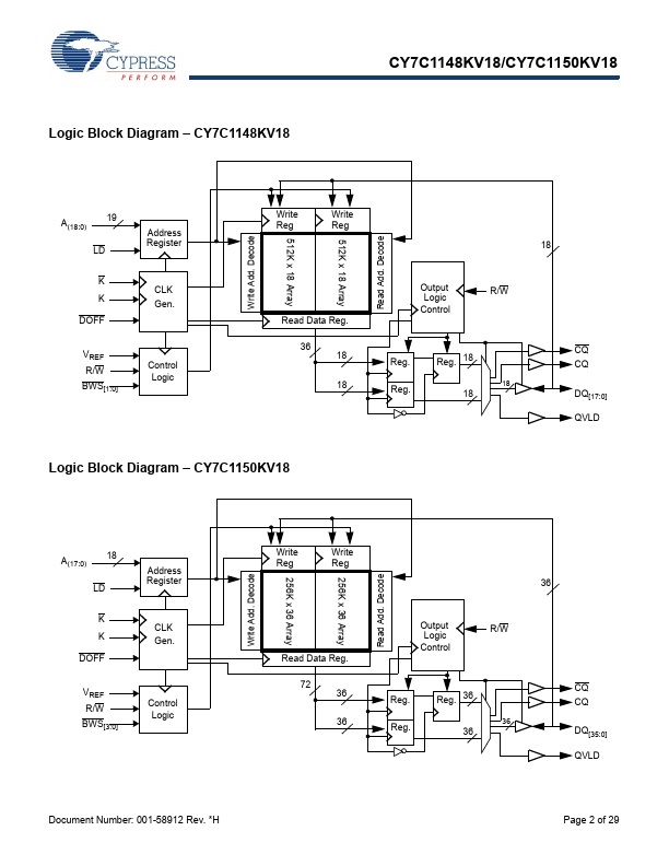
Datasheet4U Logo Datasheet4U.com

CY7C1148KV18 - 18-Mbit DDR II+ SRAM Two-Word Burst Architecture

Datasheet Summary

Features

  • 18-Mbit density (1M × 18, 512K × 36).
  • 450-MHz clock for high bandwidth.
  • Two-word burst for reducing address bus frequency.
  • Double data rate (DDR) interfaces (data transferred at 900 MHz) at 450 MHz.
  • Available in 2.0 clock cycle latency.
  • Two input clocks (K and K) for precise DDR timing.
  • SRAM uses rising edges only.
  • Echo clocks (CQ and CQ) simplify data capture in high-speed systems.
  • Data valid pin (QVLD) to indicate valid data on the output.
  • Syn.

📥 Download Datasheet

Datasheet preview – CY7C1148KV18

Datasheet Details

Part number CY7C1148KV18
Manufacturer Cypress Semiconductor
File Size 610.31 KB
Description 18-Mbit DDR II+ SRAM Two-Word Burst Architecture
Datasheet download datasheet CY7C1148KV18 Datasheet
Additional preview pages of the CY7C1148KV18 datasheet.
Other Datasheets by Cypress Semiconductor

Full PDF Text Transcription

Click to expand full text
CY7C1148KV18/CY7C1150KV18 18-Mbit DDR II+ SRAM Two-Word Burst Architecture (2.0 Cycle Read Latency) 18-Mbit DDR II+ SRAM Two-Word Burst Architecture (2.0 Cycle Read Latency) Features ■ 18-Mbit density (1M × 18, 512K × 36) ■ 450-MHz clock for high bandwidth ■ Two-word burst for reducing address bus frequency ■ Double data rate (DDR) interfaces (data transferred at 900 MHz) at 450 MHz ■ Available in 2.0 clock cycle latency ■ Two input clocks (K and K) for precise DDR timing ❐ SRAM uses rising edges only ■ Echo clocks (CQ and CQ) simplify data capture in high-speed systems ■ Data valid pin (QVLD) to indicate valid data on the output ■ Synchronous internally self-timed writes ■ DDR II+ operates with 2.
Published: |