Datasheet4U Logo Datasheet4U.com

CY7C1370B - (CY7C1370B / CY7C1372B) 512K X 36/1M X 18 Pipelined SRAM

General Description

The CY7C1370B and CY7C1372B SRAMs are designed to eliminate dead cycles when transitions from Read to Write or vice versa.

These SRAMs are optimized for 100 percent bus utilization and achieve Zero Bus Latency.

Key Features

  • Zero Bus Latency, no dead cycles between Write and Read cycles.
  • Fast clock speed: 200, 167, 150, and 133 MHz.
  • Fast access time: 3.0, 3.4, 3.8, and 4.2 ns.
  • Internally synchronized registered outputs eliminate the need to control OE.
  • Single 3.3V.
  • 5% and +10% power supply VDD.
  • Separate VDDQ for 3.3V or 2.5V I/O.
  • Single WE (Read/Write) control pin.
  • Positive clock-edge triggered address, data, and control signal register.

📥 Download Datasheet

Full PDF Text Transcription (Reference)

The following content is an automatically extracted verbatim text from the original manufacturer datasheet and is provided for reference purposes only.

View original datasheet text
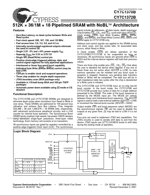
CY7C1370B CY7C1372B 512K × 36/1M × 18 Pipelined SRAM with NoBL Architecture Features • Zero Bus Latency, no dead cycles between Write and Read cycles • Fast clock speed: 200, 167, 150, and 133 MHz • Fast access time: 3.0, 3.4, 3.8, and 4.2 ns • Internally synchronized registered outputs eliminate the need to control OE • Single 3.3V –5% and +10% power supply VDD • Separate VDDQ for 3.3V or 2.