CY7C1442AV33 Description
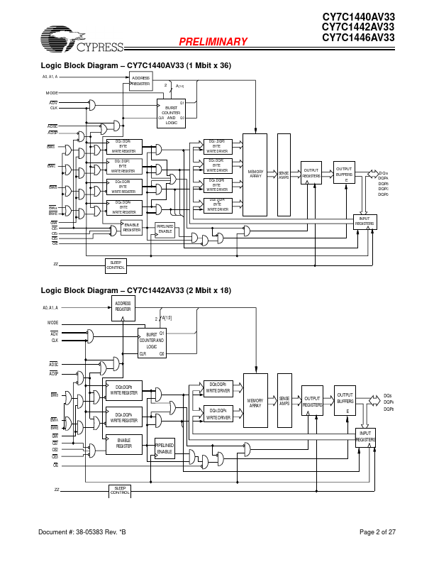
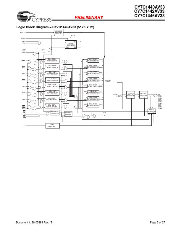
All synchronous inputs are gated by registers controlled by a positive-edge-triggered Clock Input (CLK). The synchronous inputs include all addresses, all data inputs, address-pipelining Chip Enable (CE1), depth-expansion Chip Enables (CE2 and CE3[2]), Burst Control inputs (ADSC, ADSP, and ADV), Write Enables (BWX and BWE), and Global Write (GW). Asynchronous inputs include the Output Enable (OE) and the ZZ pin.
CY7C1442AV33 Key Features
- Supports bus operation up to 250 MHz
- Available speed grades are 250, 200,167 MHz
- Registered inputs and outputs for pipelined operation
- 3.3V core power supply
- 2.5V/3.3V I/O operation
- Fast clock-to-output times
- 2.6 ns (for 250-MHz device)
- 3.2 ns (for 200-MHz device)
- 3.4 ns (for 167-MHz device)
- Provide high-performance 3-1-1-1 access rate