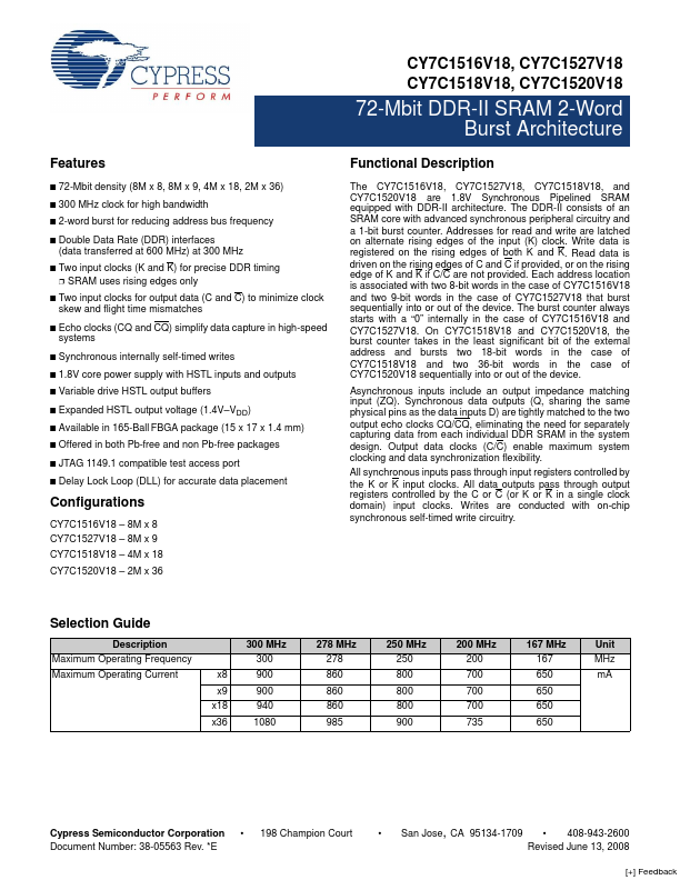
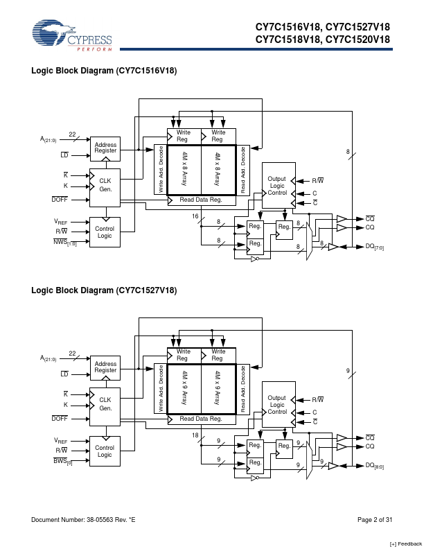
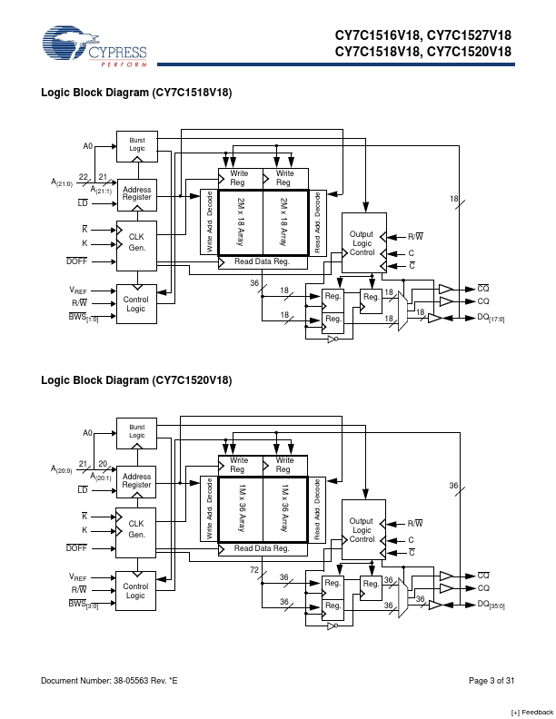
CY7C1518V18 Datasheet Text
CY7C1516V18, CY7C1527V18 CY7C1518V18, CY7C1520V18
72-Mbit DDR-II SRAM 2-Word Burst Architecture
Features
- 72-Mbit density (8M x 8, 8M x 9, 4M x 18, 2M x 36)
- 300 MHz clock for high bandwidth
- 2-word burst for reducing address bus frequency
- Double Data Rate (DDR) interfaces
(data transferred at 600 MHz) at 300 MHz
- Two input clocks (K and K) for precise DDR timing
- SRAM uses rising edges only
- Two input clocks for output data (C and C) to minimize clock skew and flight time mismatches
- Echo clocks (CQ and CQ) simplify data capture in high-speed systems
- Synchronous internally self-timed writes
- 1.8V core power supply with HSTL inputs and outputs
- Variable drive HSTL output buffers
- Expanded HSTL output voltage (1.4V- VDD)
- Available in 165-Ball FBGA package (15 x 17 x 1.4 mm)
- Offered in both Pb-free and non Pb-free packages
- JTAG 1149.1 patible test access port
- Delay Lock Loop (DLL) for accurate data...