Datasheet4U Logo Datasheet4U.com

CY7C1613KV18 - 144-Mbit QDR II SRAM Four-Word Burst Architecture

Datasheet Summary

Features

  • Separate independent read and write data ports.
  • Supports concurrent transactions.
  • 333 MHz clock for high bandwidth.
  • Four-word burst for reducing address bus frequency.
  • Double Data Rate (DDR) interfaces on both read and write ports (data transferred at 666 MHz) at 333 MHz.
  • Two input clocks (K and K) for precise DDR timing.
  • SRAM uses rising edges only.
  • Two input clocks for output data (C and C) to minimize clock skew and flight time mismatches.
  • Echo cl.

📥 Download Datasheet

Datasheet preview – CY7C1613KV18

Datasheet Details

Part number CY7C1613KV18
Manufacturer Cypress Semiconductor
File Size 586.14 KB
Description 144-Mbit QDR II SRAM Four-Word Burst Architecture
Datasheet download datasheet CY7C1613KV18 Datasheet
Additional preview pages of the CY7C1613KV18 datasheet.
Other Datasheets by Cypress Semiconductor

Full PDF Text Transcription

Click to expand full text
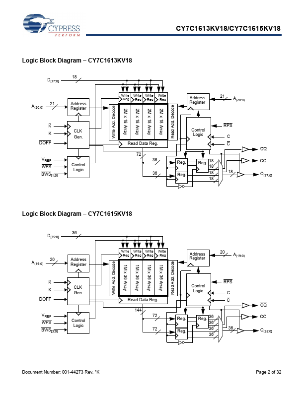
CY7C1613KV18/CY7C1615KV18 144-Mbit QDR® II SRAM Four-Word Burst Architecture 144-Mbit QDR® II SRAM Four-Word Burst Architecture Features ■ Separate independent read and write data ports ❐ Supports concurrent transactions ■ 333 MHz clock for high bandwidth ■ Four-word burst for reducing address bus frequency ■ Double Data Rate (DDR) interfaces on both read and write ports (data transferred at 666 MHz) at 333 MHz ■ Two input clocks (K and K) for precise DDR timing ❐ SRAM uses rising edges only ■ Two input clocks for output data (C and C) to minimize clock skew and flight time mismatches ■ Echo clocks (CQ and CQ) simplify data capture in high speed systems ■ Single multiplexed address input bus latches address inputs for read and write ports ■ Separate port selects for depth expansion ■ Sync
Published: |