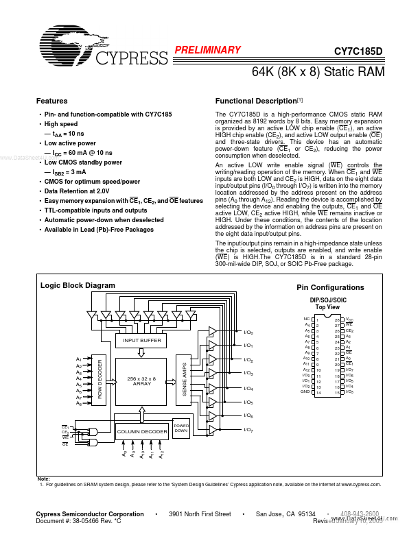
• Part: CY7C185D
  • Description: 64K (8K x 8) Static RAM
  • Manufacturer: Cypress
  • Size: 219.29 KB
Download CY7C185D Datasheet PDF
Cypress
CY7C185D
CY7C185D is 64K (8K x 8) Static RAM manufactured by Cypress.
PRELIMINARY 64K (8K x 8) Static RAM Features - Pin- and function-patible with CY7C185 - High speed - t AA = 10 ns - Low active power .. Functional Description[1] The CY7C185D is a high-performance CMOS static RAM organized as 8192 words by 8 bits. Easy memory expansion is provided by an active LOW chip enable (CE1), an active HIGH chip enable (CE2), and active LOW output enable (OE) and three-state drivers. This device has an automatic power-down feature (CE1 or CE2), reducing the power consumption when deselected. An active LOW write enable signal (WE) controls the writing/reading operation of the memory. When CE1 and WE inputs are both LOW and CE2 is HIGH, data on the eight data input/output pins (I/O0 through I/O7) is written into the memory location addressed by the address present on the address pins (A0 through A12). Reading the device is acplished by selecting the device and enabling the outputs, CE1 and OE active LOW, CE2 active HIGH, while WE remains inactive or HIGH. Under these conditions, the contents of the location addressed by the information on address pins are present on the eight data input/output pins. The input/output pins remain in a high-impedance state unless the chip is selected, outputs are enabled, and write enable (WE) is HIGH.The CY7C185D is in a standard 28-pin 300-mil-wide DIP, SOJ, or SOIC Pb-Free package. - ICC = 60 m A @ 10 ns - Low CMOS standby power - ISB2 = 3 m A - CMOS for optimum speed/power - Data Retention at 2.0V - Easy memory expansion with CE1, CE2, and OE Features - TTL-patible inputs and outputs - Automatic power-down when deselected - Available in Lead (Pb)-Free Packages Logic Block Diagram Pin Configurations DIP/SOJ/SOIC Top View NC A4 A5 A6 A7 A8 A9 A10 A11 A12 I/O0 I/O1 I/O2 GND 1 2 3 4 5 6 7 8 9 10 11 12 13 14 28 27 26 25 24 23 22 21 20 19 18 17 16 15 VCC WE CE2 A3 A2 A1 OE A0 CE1 I/O7 I/O6 I/O5 I/O4 I/O3 I/O0 INPUT BUFFER I/O1 A1 A2 A3 A4 A5 A6 A7 A8 ROW DECODER SENSE...