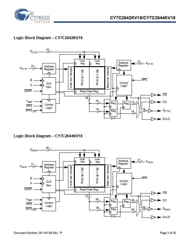
Datasheet4U Logo Datasheet4U.com

CY7C2644KV18 - 144-Mbit QDR II+ SRAM Two-Word Burst Architecture

This page provides the datasheet information for the CY7C2644KV18, a member of the CY7C2642KV18 144-Mbit QDR II+ SRAM Two-Word Burst Architecture family.

Datasheet Summary

Features

  • Separate independent read and write data ports.
  • Supports concurrent transactions.
  • 333-MHz clock for high bandwidth.
  • Two-word burst for reducing address bus frequency.
  • Double data rate (DDR) interfaces on both read and write ports (data transferred at 666 MHz) at 333 MHz.
  • Available in 2.0-clock cycle latency.
  • Two input clocks (K and K) for precise DDR timing.
  • SRAM uses rising edges only.
  • Echo clocks (CQ and CQ) simplify data capture in high-speed sys.

📥 Download Datasheet

Datasheet preview – CY7C2644KV18

Datasheet Details

Part number CY7C2644KV18
Manufacturer Cypress Semiconductor
File Size 607.25 KB
Description 144-Mbit QDR II+ SRAM Two-Word Burst Architecture
Datasheet download datasheet CY7C2644KV18 Datasheet
Additional preview pages of the CY7C2644KV18 datasheet.
Other Datasheets by Cypress Semiconductor

Full PDF Text Transcription

Click to expand full text
CY7C2642KV18/CY7C2644KV18 144-Mbit QDR® II+ SRAM Two-Word Burst Architecture (2.0 Cycle Read Latency) with ODT 144-Mbit QDR® II+ SRAM Two-Word Burst Architecture (2.0 Cycle Read Latency) with ODT Features ■ Separate independent read and write data ports ❐ Supports concurrent transactions ■ 333-MHz clock for high bandwidth ■ Two-word burst for reducing address bus frequency ■ Double data rate (DDR) interfaces on both read and write ports (data transferred at 666 MHz) at 333 MHz ■ Available in 2.
Published: |