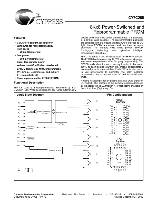
Datasheet Details
| Part number | CY7C266 |
|---|---|
| Manufacturer | Cypress (now Infineon) |
| File Size | 261.10 KB |
| Description | 8Kx8 Power-Switched and Reprogrammable PROM |
| Datasheet | CY7C266_CypressSemiconductor.pdf |
|
|
|
Overview: 1CY7C266 CY7C266 8Kx8 Power-Switched and Reprogrammable PROM.
| Part number | CY7C266 |
|---|---|
| Manufacturer | Cypress (now Infineon) |
| File Size | 261.10 KB |
| Description | 8Kx8 Power-Switched and Reprogrammable PROM |
| Datasheet | CY7C266_CypressSemiconductor.pdf |
|
|
|
The CY7C266 is a high-performance 8192-word by 8-bit CMOS PROM.
When deselected, the CY7C266 automatically Logic Block Diagram O7 A0 A1 A2 A3 A4 A5 A6 A7 A8 A9 A10 A11 A12 POWER DOWN O1 O2 COLUMN ADDRESS O3 ADDRESS DECODER O4 O5 ROW ADDRESS PROGRAMMABLE ARRAY O6 MULTIPLEXER Pin Configurations CerDIP Top View VCC A12 A7 A6 A5 A4 A3 A2 A1 A0 O0 O1 O2 GND 1 2 3 4 5 6 7 8 9 7C266 10 11 12 13 14 28 27 26 25 24 23 22 21 20 19 18 17 16 15 VCC VCC NC A8 A9 A11 OE A10 CE O7 O6 O5 O4 O3 LCC Top View A7 A 12 VCC NC VCC VCC NC A6 A5 A4 A3 A2 A1 A0 NC O0
| Part Number | Description |
|---|---|
| CY7C2663KV18 | 144-Mbit QDR II+ SRAM Four-Word Burst Architecture |
| CY7C2665KV18 | 144-Mbit QDR II+ SRAM Four-Word Burst Architecture |
| CY7C261 | 8K x 8 Power-Switched and Reprogrammable PROM |
| CY7C263 | 8K x 8 Power-Switched and Reprogrammable PROM |
| CY7C264 | 8K x 8 Power-Switched and Reprogrammable PROM |
| CY7C2642KV18 | 144-Mbit QDR II+ SRAM Two-Word Burst Architecture |
| CY7C2644KV18 | 144-Mbit QDR II+ SRAM Two-Word Burst Architecture |
| CY7C265 | 8K x 8 Registered PROM |
| CY7C2670KV18 | 144-Mbit DDR II+ SRAM Two-Word Burst Architecture |
| CY7C2163KV18 | 18-Mbit QDR II+ SRAM Four-Word Burst Architecture |