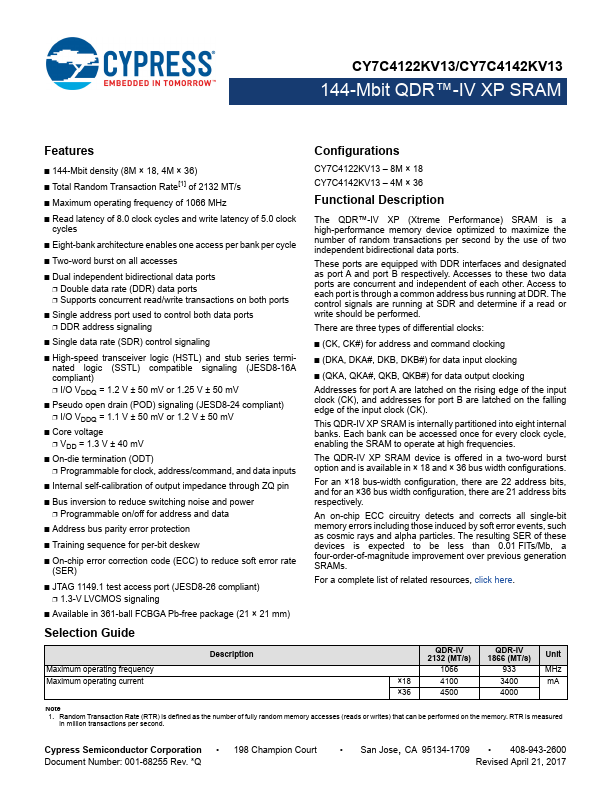
Datasheet4U Logo Datasheet4U.com

CY7C4122KV13 - 144-Mbit QDR-IV XP SRAM

General Description

The QDR™-IV XP (Xtreme Performance) SRAM is a high-performance memory device optimized to maximize the number of random transactions per second by the use of two independent bidirectional data ports.

These ports are equipped with DDR interfaces and designated as port A and port B respectively.

Key Features

  • e 144-Mbit QDR™-IV XP SRAM Configurations.
  • 144-Mbit density (8M × 18, 4M × 36).
  • Total Random Transaction Rate[1] of 2132 MT/s.
  • Maximum operating frequency of 1066 MHz.
  • Read latency of 8.0 clock cycles and write latency of 5.0 clock cycles.
  • Eight-bank architecture enables one access per bank per cycle.
  • Two-word burst on all accesses.
  • Dual independent bidirectional data ports.
  • Double data rate (DDR) data ports.
  • Supports concurrent read/write transacti.

📥 Download Datasheet

Full PDF Text Transcription (Reference)

The following content is an automatically extracted verbatim text from the original manufacturer datasheet and is provided for reference purposes only.

View original datasheet text
CY7C4122KV13/CY7C4142KV13 144-Mbit QDR™-IV XP SRAM Features e 144-Mbit QDR™-IV XP SRAM Configurations ■ 144-Mbit density (8M × 18, 4M × 36) ■ Total Random Transaction Rate[1] of 2132 MT/s ■ Maximum operating frequency of 1066 MHz ■ Read latency of 8.0 clock cycles and write latency of 5.0 clock cycles ■ Eight-bank architecture enables one access per bank per cycle ■ Two-word burst on all accesses ■ Dual independent bidirectional data ports ❐ Double data rate (DDR) data ports ❐ Supports concurrent read/write transactions on both ports ■ Single address port used to control both data ports ❐ DDR address signaling ■ Single data rate (SDR) control signaling ■ High-speed transceiver logic (HSTL) and stub series terminated logic (SSTL) compatible signaling (JESD8-16A compliant) ❐ I/O VDDQ = 1.