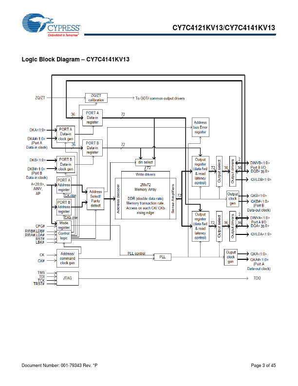
CY7C4141KV13 Description
CY7C4121KV13/CY7C4141KV13 144-Mbit QDR™-IV HP SRAM 144-Mbit QDR™-IV HP SRAM.
CY7C4141KV13 Key Features
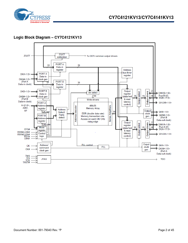
- 144-Mbit density (8M ×18, 4M ×36)
- Total Random Transaction Rate [1] of 1334 MT/s
- Maximum operating frequency of 667 MHz
- Read latency of 5.0 clock cycles and write latency of 3.0 clock cycles
- Two-word burst on all accesses
- Dual independent bidirectional data ports
- Double data rate (DDR) data ports
- Supports concurrent read/write transactions on both ports
- Single address port used to control both data ports
- DDR address signaling