Datasheet4U Logo Datasheet4U.com

CY7C454 - (CY7C451 - CY7C454) Cascadable Colcked FIFOs

Download the CY7C454 datasheet PDF. This datasheet also covers the CY7C451 variant, as both devices belong to the same (cy7c451 - cy7c454) cascadable colcked fifos family and are provided as variant models within a single manufacturer datasheet.

Description

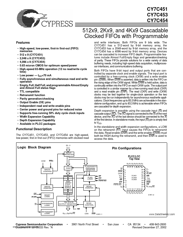
The CY7C451, CY7C453, and CY7C454 are high-speed, low-power, first-in first-out (FIFO) memories with clocked read Logic Block Diagram D0 8 Pin Configurations INPUT REGISTER CKW ENW FLAG/PARITY PROGRAM REGISTER PLCC/LCC Top View D0 D1 D2 D3 D4 D5 D6 PARITY WRITE CONTROL FLAG LOGIC R

Features

  • High-speed, low-power, first-in first-out (FIFO) memories.
  • 512 x 9 (CY7C451).
  • 2,048 x 9 (CY7C453).
  • 4,096 x 9 (CY7C454).
  • 0.65 micron CMOS for optimum speed/power.
  • High-speed 83-MHz operation (12 ns read/write cycle time).
  • Low power.
  • ICC=70 mA.
  • Fully asynchronous and simultaneous read and write operation.
  • Empty, Full, Half Full, and programmable Almost Empty and Almost Full status flags.
  • TTL compati.

📥 Download Datasheet

Note: The manufacturer provides a single datasheet file (CY7C451_CypressSemiconductor.pdf) that lists specifications for multiple related part numbers.

Full PDF Text Transcription

Click to expand full text
54 CY7C451 CY7C453 CY7C454 512x9, 2Kx9, and 4Kx9 Cascadable Clocked FIFOs with Programmable Features • High-speed, low-power, first-in first-out (FIFO) memories • 512 x 9 (CY7C451) • 2,048 x 9 (CY7C453) • 4,096 x 9 (CY7C454) • 0.
Published: |