CYM1481
CYM1481 is 2048k X 8 SRAM Module manufactured by Cypress.
- Part of the CYM1471 comparator family.
- Part of the CYM1471 comparator family.
1CY M14 81 fax id: 2006
..
CYM1471 CYM1481
1024K x 8 SRAM Module 2048K x 8 SRAM Module
Features
- High-density 8-/16-megabit SRAM modules
- High-speed CMOS SRAMs
- Access time of 70 ns
- Low active power
- 605 mW (max.), 2M x 8
- Double-sided SMD technology
- TTL-patible inputs and outputs
- Small footprint SIP
- PCB layout area of 0.72 sq. in.
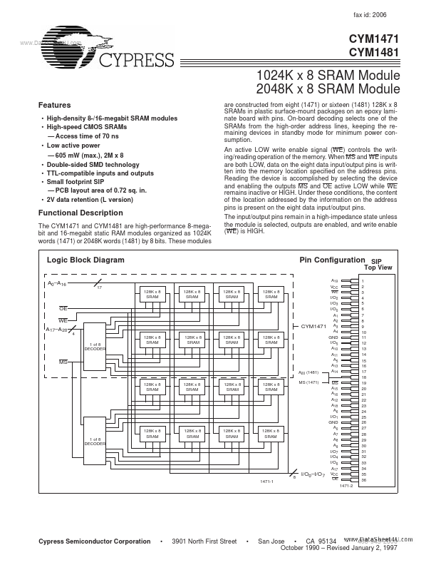
- 2V data retention (L version) are constructed from eight (1471) or sixteen (1481) 128K x 8 SRAMs in plastic surface-mount packages on an epoxy laminate board with pins. On-board decoding selects one of the SRAMs from the high-order address lines, keeping the remaining devices in standby mode for minimum power consumption....