CYWB0224ABM Overview
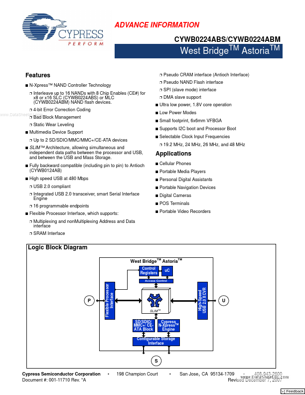
ADVANCE INFORMATION CYWB0224ABS/CYWB0224ABM TM TM West Bridge Astoria.
CYWB0224ABM Key Features
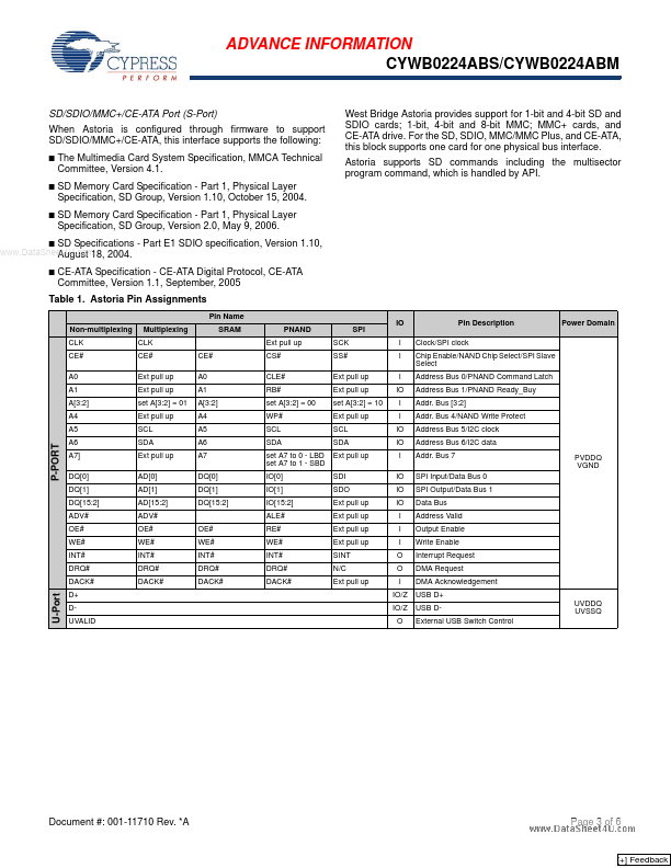
- Pseudo CRAM interface (Antioch Interface) Pseudo NAND Flash interface SPI (slave mode) interface DMA slave support
- Interleave up to 16 NANDs with 8 Chip Enables (CE#) for x8 or x16 SLC (CYWB0224ABS) or MLC (CYWB0224ABM) NAND flash devi
- Up to 2 SD/SDIO/MMC/MMC+/CE-ATA devices
- SLIM™ Architecture, allowing simultaneous and independent data paths between the processor and USB, and between the USB
- 19.2 MHz, 24 MHz, 26 MHz, and 48 MHz