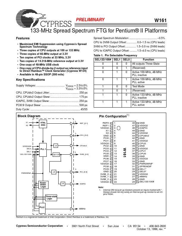
Datasheet4U Logo Datasheet4U.com

W161 - 133-MHz Spread Spectrum FTG

Description

CPU Clock Outputs 0 through 2: CPU clock outputs.

Their output voltage swing is controlled by voltage applied to VDDQ2.

PCI Clock Outputs 0 through 9: Output voltage swing is controlled by voltage applied to VDDQ3.

Features

  • Maximized EMI Suppression using Cypress’s Spread Spectrum Technology.
  • Three copies of CPU outputs at 100 or 133 MHz.
  • Three copies of 66-MHz output at 3.3V.
  • Ten copies of PCI clocks at 33 MHz, 3.3V.
  • Two copies of 14.318-MHz reference output at 3.3V.
  • One copy of 48-MHz USB clock.
  • One copy of CPU-divide-by-2 output as reference input to Direct Rambus™ Clock Generator (Cypress W134).
  • Available in 48-pin SSOP (300 mils) Spread S.

📥 Download Datasheet

Datasheet preview – W161

Datasheet Details

Part number W161
Manufacturer Cypress
File Size 117.41 KB
Description 133-MHz Spread Spectrum FTG
Datasheet download datasheet W161 Datasheet
Additional preview pages of the W161 datasheet.
Other Datasheets by Cypress Semiconductor

Full PDF Text Transcription

Click to expand full text
PRELIMINARY W161 133-MHz Spread Spectrum FTG for Pentium® II Platforms Features • Maximized EMI Suppression using Cypress’s Spread Spectrum Technology • Three copies of CPU outputs at 100 or 133 MHz • Three copies of 66-MHz output at 3.3V • Ten copies of PCI clocks at 33 MHz, 3.3V • Two copies of 14.318-MHz reference output at 3.3V • One copy of 48-MHz USB clock • One copy of CPU-divide-by-2 output as reference input to Direct Rambus™ Clock Generator (Cypress W134) • Available in 48-pin SSOP (300 mils) Spread Spectrum Modulation:..................................... –0.5% CPU to 3V66 Output Offset: ............. 0.0–1.5 ns (CPU leads) 3V66 to PCI Output Offset:.............. 1.5–3.0 ns (3V66 leads) CPU to IOAPIC Output Offset: ......... 1.5–4.0 ns (CPU leads) Table 1.
Published: |