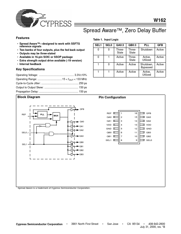
W162 Overview
The output signals QA0:3 through QB0:3 will be synchronized to this signal unless the device is programmed to bypass the PLL. This signal is used as the feedback internally to establish the propagation delay of nearly 0. The frequency of the signals provided by these pins is equal to the signal connected to REF.
W162 Key Features
- Spread Aware™-designed to work with SSFTG reference signals
- Two banks of four outputs, plus the fed back output
- Outputs may be three-stated
- Available in 16-pin SOIC or SSOP package
- Extra strength output drive available (-19 version)
- 3.3V±10% Operating Range
- 15 < fOUT < 133 MHz Cycle-to-Cycle Jitter
- 250 ps Output to Output Skew
- 150 ps Propagation Delay
- 150 ps