CY29940 Description
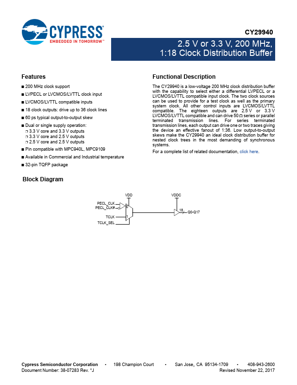
The CY29940 is a low-voltage 200 MHz clock distribution buffer with the capability to select either a differential LVPECL or a LVCMOS/LVTTL patible input clock. The two clock sources can be used to provide for a test clock as well as the primary system clock. All other control inputs are LVCMOS/LVTTL patible.
CY29940 Key Features
- 200 MHz clock support
- LVPECL or LVCMOS/LVTTL clock input
- LVCMOS/LVTTL patible inputs
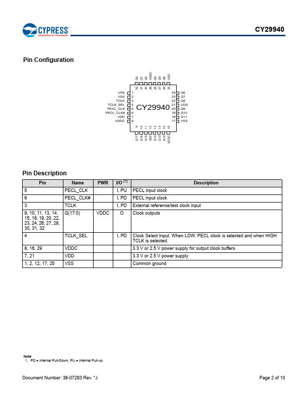
- 18 clock outputs: drive up to 36 clock lines
- 60 ps typical output-to-output skew
- Dual or single supply operation
- 3.3 V core and 3.3 V outputs
- 3.3 V core and 2.5 V outputs
- 2.5 V core and 2.5 V outputs
- Pin patible with MPC940L, MPC9109