CY2CC910 Description
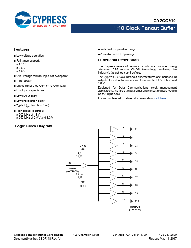
The Cypress series of network circuits are produced using advanced 0.35 micron CMOS technology, achieving the industry’s fastest logic and buffers. The Cypress CY2CC910 fanout buffer.
CY2CC910 Key Features
- Low voltage operation
- Full range support
- Over voltage tolerant input hot swappable
- 1:10 Fanout
- Drives either a 50-Ohm or 75-Ohm load
- Low input capacitance
- Low output skew
- Low propagation delay
- Typical (tpd less than 4 ns)
- High speed operation