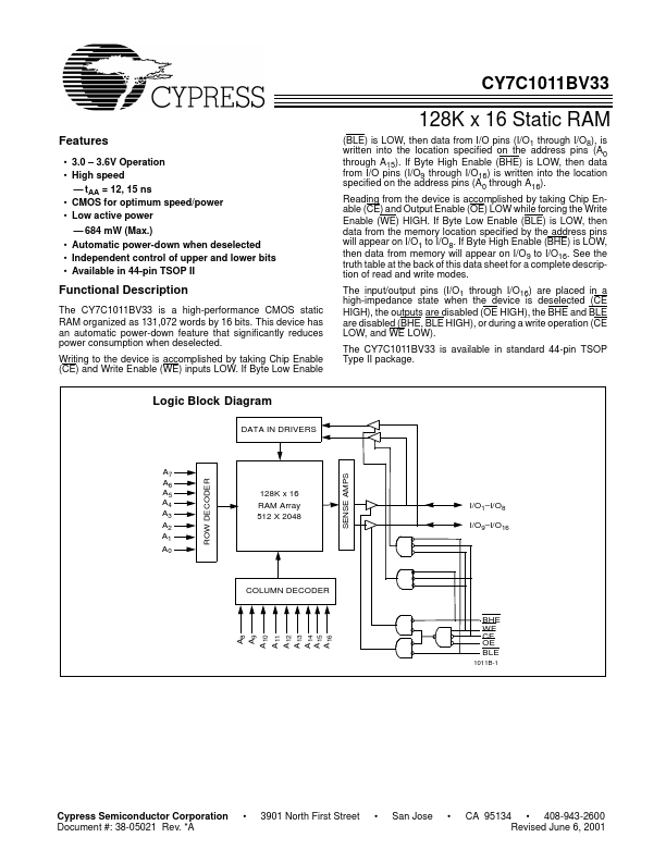
CY7C1011BV33 Description
The input/output pins (I/O1 through I/O16) are placed in a high-impedance state when the device is deselected (CE HIGH), the outputs are disabled (OE HIGH), the BHE and BLE are disabled (BHE, BLE HIGH), or during a write operation (CE LOW, and WE LOW). The CY7C1011BV33 is available in standard 44-pin TSOP Type II package. Functional Description The CY7C1011BV33 is a high-performance CMOS static RAM organized as...
CY7C1011BV33 Key Features
- 3.6V Operation
- High speed
- tAA = 12, 15 ns
- CMOS for optimum speed/power
- Low active power
- 684 mW (Max.)
- Automatic power-down when deselected
- Independent control of upper and lower bits
- 3901 North First Street
- San Jose