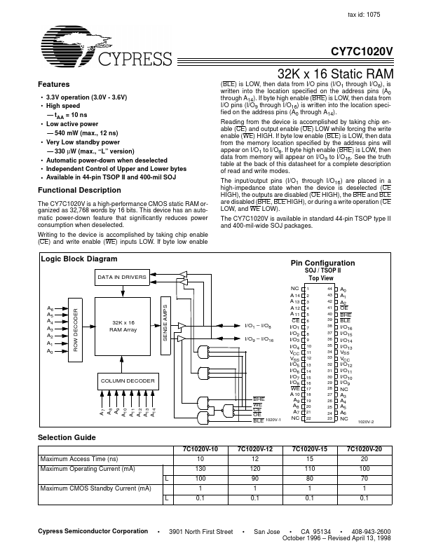
CY7C1020V Description
The input/output pins (I/O1 through I/O16) are placed in a high-impedance state when the device is deselected (CE HIGH), the outputs are disabled (OE HIGH), the BHE and BLE are disabled (BHE, BLE HIGH), or during a write operation (CE LOW, and WE LOW). The CY7C1020V is available in standard 44-pin TSOP type II and 400-mil-wide SOJ packages. Functional Description The CY7C1020V is a high-performance CMOS static RAM...
CY7C1020V Key Features
- 3.3V operation (3.0V
- High speed
- tAA = 10 ns
- Low active power
- 540 mW (max., 12 ns)
- Very Low standby power
- 330 µW (max., “L” version)
- Automatic power-down when deselected
- Independent Control of Upper and Lower bytes