2SD882
Description
Designed for use in output stage of 1W audio amplifier, voltage regulator, DC-DC converter and relay driver.
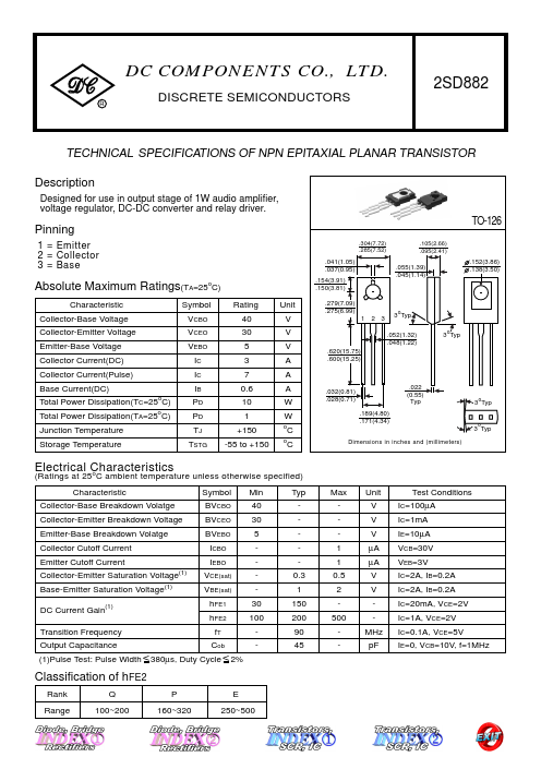
Pinning
1 = Emitter 2 = Collector 3 = Base
Absolute Maximum Ratings(TA=25o C)
Characteristic Collector-Base Voltage Collector-Emitter Voltage Emitter-Base Voltage Collector Current(DC) Collector Current(Pulse) Base Current(DC) Total Power Dissipation(TC=25o C) Total Power Dissipation(TA=25o C) Junction Temperature Storage Temperature
Symbol VCBO VCEO VEBO IC IC IB PD PD TJ TSTG
Rating Unit
+150 o C
-55 to +150 o C
TO-126
.304(7.72) .285(7.52)
.041(1.05) .037(0.95)
.154(3.91) .150(3.81)
.105(2.66) .095(2.41)
.055(1.39) .045(1.14)
.152(3.86) .138(3.50)
.279(7.09)
.275(6.99) 1 23
3o Typ
.620(15.75) .600(15.25)
.052(1.32) .048(1.22)
3o Typ
.032(0.81) .028(0.71)
.189(4.80) .171(4.34)
.022
(0.55) Typ
Dimensions in inches and (millimeters)
3o Typ 3o Typ
Electrical Characteristics
(Ratings at 25o C ambient...