2SD882D
Description
Designed for use in output stage of 1W audio amplifier, voltage regulator, DC-DC converter and relay driver.
Pinning
1 = Emitter 2 = Collector 3 = Base
.163(4.12) .153(3.87) .044(1.12) .034(0.87) .060(1.52) .050(1.27)
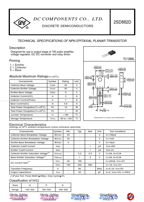
TO-126ML
.146(3.70) .136(3.44)
Absolute Maximum Ratings(TA=25o C)
Characteristic Collector-Base Voltage Collector-Emitter Voltage Emitter-Base Voltage Collector Current(DC)
..
.148(3.75) .138(3.50)
Symbol VCBO VCEO VEBO IC IC IB o
Rating 40 30 5 3 7 0.6 10 1 +150 -55 to +150
Unit V V V A A A W W o o
.123(3.12) .113(2.87)
.300(7.62) .290(7.37) 1 2 3 .084(2.12) .074(1.87) .056(1.42) .046(1.17) .033(0.84) .027(0.68) .180 Typ (4.56) .090 Typ (2.28) .084(2.14) .074(1.88)
Collector Current(Pulse) Base Current(DC)
.591(15.0) .551(14.0)
Total Power Dissipation(TC=25 C) Total Power Dissipation(TA=25 C) Junction Temperature Storage Temperature o
PD PD TJ TSTG
.027(0.69) .017(0.43)
Dimensions in inches and (millimeters)
Electrical Characteristics o
Characteristic
(Ratings at 25 C ambient temperature unless...