DESCRIPTION
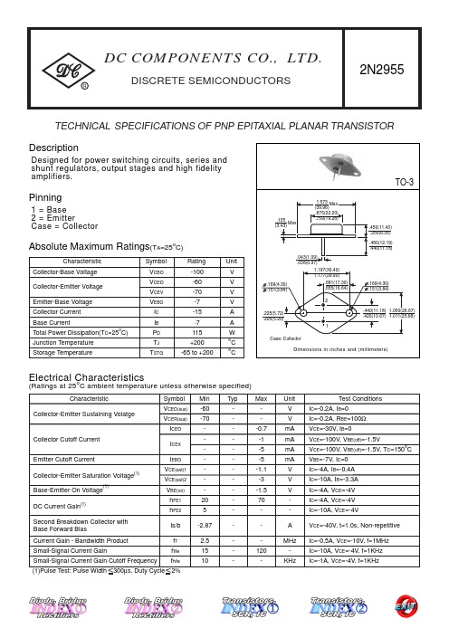
Designed for power switching circuits, series and shunt regulators, output stages and high fidelity amplifiers. TO-3 1.573 Max (39.96) .875(22.23) .759(19.28) .450(11.43) .250(6.35) .480(12.19) .440(11.18) Pinning 1 = Base 2 = Emitter Case = Collector .135 Max (3.43) ABSOLUTE MAXIMUM RATINGS
(TA=25oC) Characteristic Collector-Base Voltage Collector-Emitter Voltage Emitter-Base Voltage Collector Current Base Current Total Power Dissipation(TC=25 C) Junction Temperature Storage Temperature o Symbol VCBO VCEO VCEV VEBO IC IB PD TJ TSTG Rating -100 -60 -70 -7 -15 -7 Unit V V V V A A W o o .225(5.72) .205(5.20) .169(4.30) .151(3.84) .043(1.09) .038(0.97) 1.197(30.40) 1.177(29.90) .681(17.30) .655(16.64) 2 .440(11.18) 1.050(26.67) .420(10.67) 1.011(25.68) 1 Case: Collector .169(4.30) .151(3.84) 115 +200 -65 to +200 C C Dimensions in inches and (millimeters) ELECTRICAL CHARACTERISTICS
o Characteristic Collector-Emitter Sustaining Volatge (Ratings at 25 C ambient temperature unless... Dc Components