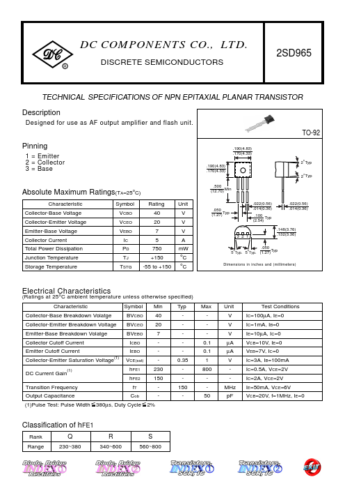
DESCRIPTION
Designed for use as AF output amplifier and flash unit. TO-92 Pinning 1 = Emitter 2 = Collector 3 = Base .190(4.83) .170(4.33) .190(4.83) .170(4.33) 2 Typ 2 Typ o o ABSOLUTE MAXIMUM RATINGS
(TA=25oC) Characteristic Collector-Base Voltage Collector-Emitter Voltage Emitter-Base Voltage Collector Current Total Power Dissipation Junction Temperature Storage Temperature Symbol VCBO VCEO VEBO IC PD TJ TSTG Rating 40 20 7 5 750 +150 -55 to +150 Unit V V V A mW o o .500 Min (12.70) .022(0.56) .014(0.36) .100 Typ (2.54) .148(3.76) .132(3.36) .022(0.56) .014(0.36) .050 Typ (1.27) 3 2 1 .050 o o 5 Typ. 5 Typ. (1.27) Typ Dimensions in inches and (millimeters) C C ELECTRICAL CHARACTERISTICS
o Characteristic (Ratings at 25 C ambient temperature unless otherwise specified) Symbol BVCBO BVCEO BVEBO ICBO IEBO (1) Min 40 20 7 230 150 2% Typ 0.35 150 - Max 0.1 0.1 1 800 50 Unit V V V µA µA V MHz pF Test Conditions IC=100µA, IE=0 IC=1mA, IB=0 IE=10µA, IC=0 VCB=10V, IE=0 VEB=7V, IC=0 IC=3A, IB=1... Dc Components