Datasheet4U Logo Datasheet4U.com

DMP1007UCB9 - P-CHANNEL MOSFET

General Description

This 3rd generation Lateral MOSFET (LD-MOS) is engineered to minimize on-state losses and switch ultra-fast, making it ideal for high efficiency power transfer.

It uses Chip-Scale Package (CSP) to increase power density by combining low thermal impedance with minimal RDS(ON) per footprint area.

Key Features

  • LD-MOS Technology with the Lowest Figure of Merit:.
  • RDS(ON) = 5.7mΩ to Minimize On-State Losses.
  • Qg = 8.2nC for Ultra-Fast Switching.
  • VGS(TH) = -0.6V Typ. for a Low Turn-On Potential.
  • CSP with Footprint 1.5mm  1.5mm.
  • Height = 0.62mm for Low Profile.
  • ESD Protection of Gate.
  • Totally Lead-Free & Fully RoHS Compliant (Notes 1 & 2).
  • Halogen and Antimony Free. “Green” Device (Note 3).
  • For automotive.

📥 Download Datasheet

Full PDF Text Transcription (Reference)

The following content is an automatically extracted verbatim text from the original manufacturer datasheet and is provided for reference purposes only.

View original datasheet text
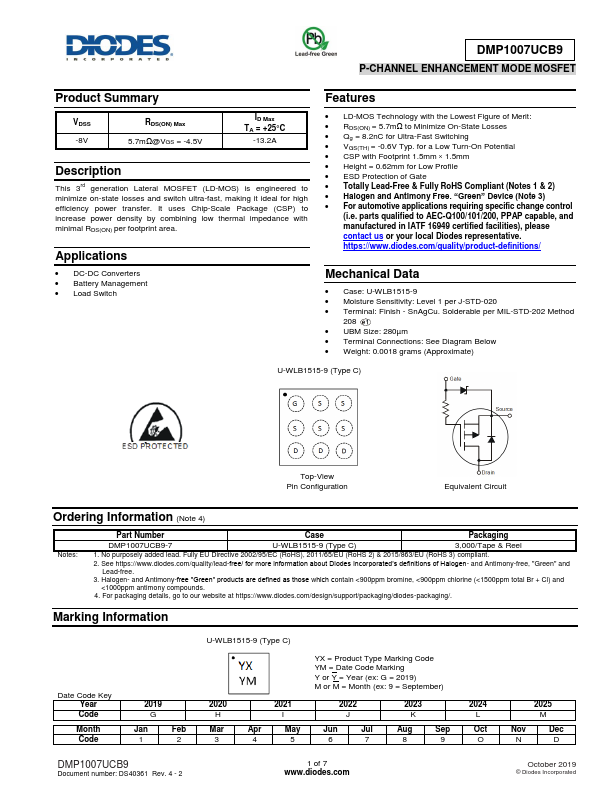
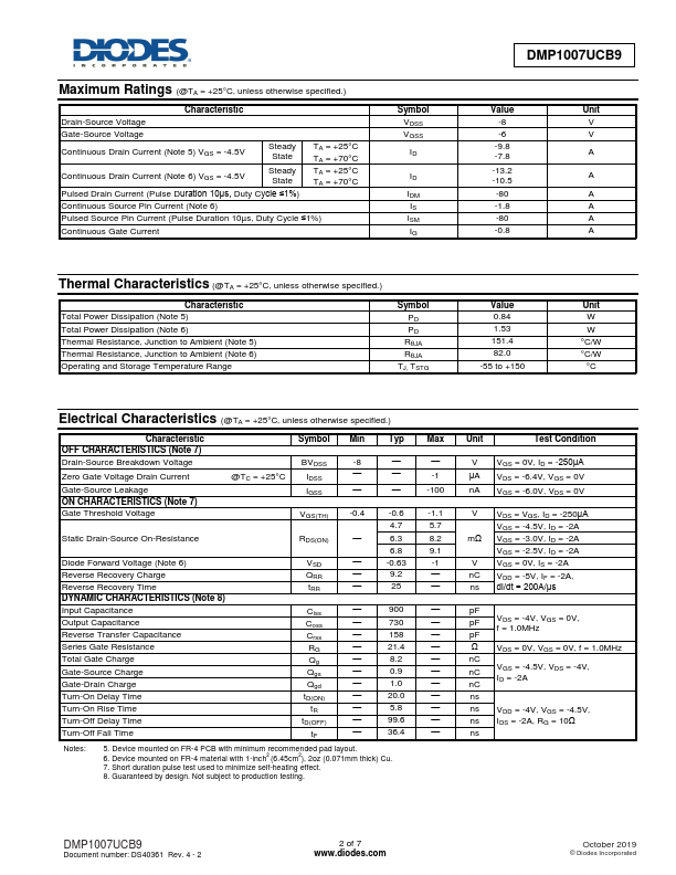
DMP1007UCB9 P-CHANNEL ENHANCEMENT MODE MOSFET Product Summary VDSS -8V RDS(ON) Max 5.7mΩ@VGS = -4.5V ID Max TA = +25°C -13.2A Description This 3rd generation Lateral MOSFET (LD-MOS) is engineered to minimize on-state losses and switch ultra-fast, making it ideal for high efficiency power transfer. It uses Chip-Scale Package (CSP) to increase power density by combining low thermal impedance with minimal RDS(ON) per footprint area. Applications  DC-DC Converters  Battery Management  Load Switch Features  LD-MOS Technology with the Lowest Figure of Merit:  RDS(ON) = 5.7mΩ to Minimize On-State Losses  Qg = 8.2nC for Ultra-Fast Switching  VGS(TH) = -0.6V Typ. for a Low Turn-On Potential  CSP with Footprint 1.5mm  1.5mm  Height = 0.