DMN31D5UFZ
DMN31D5UFZ is N-CHANNEL ENHANCEMENT MODE MOSFET manufactured by Diodes Incorporated.
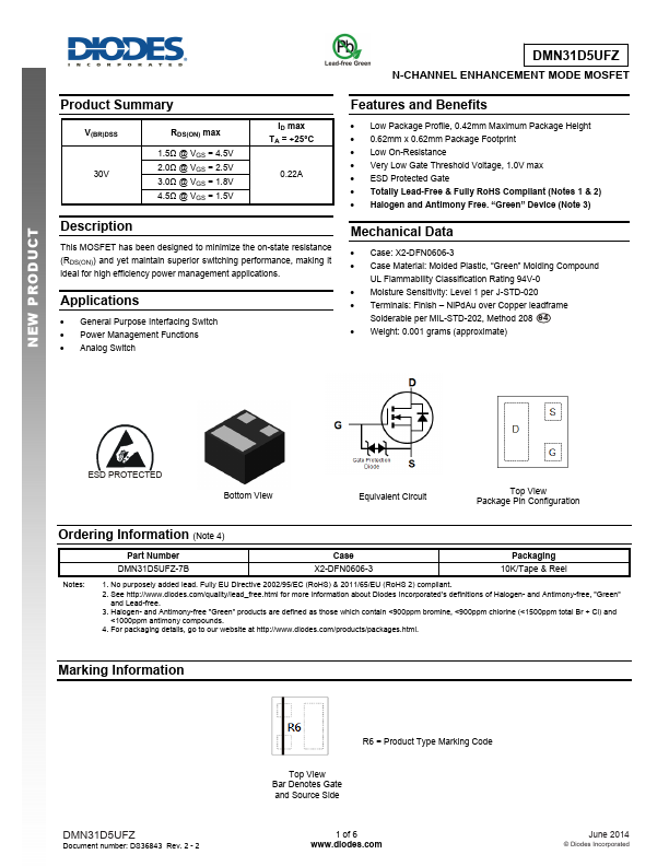
A D VNA EN CWEPDRNIOENDFWUOPCRRTMOADTUI COTN
N-CHANNEL ENHANCEMENT MODE MOSFET
Product Summary
V(BR)DSS 30V
RDS(ON) max
1.5Ω @ VGS = 4.5V 2.0Ω @ VGS = 2.5V 3.0Ω @ VGS = 1.8V 4.5Ω @ VGS = 1.5V
ID max TA = +25°C
0.22A
Description
This MOSFET has been designed to minimize the on-state resistance (RDS(ON)) and yet maintain superior switching performance, making it ideal for high efficiency power management applications.
Applications
- General Purpose Interfacing Switch
- Power Management Functions
- Analog Switch
Features and Benefits
- Low Package Profile, 0.42mm Maximum Package Height
- 0.62mm x 0.62mm Package Footprint
- Low On-Resistance
- Very Low Gate Threshold...