FEATURES
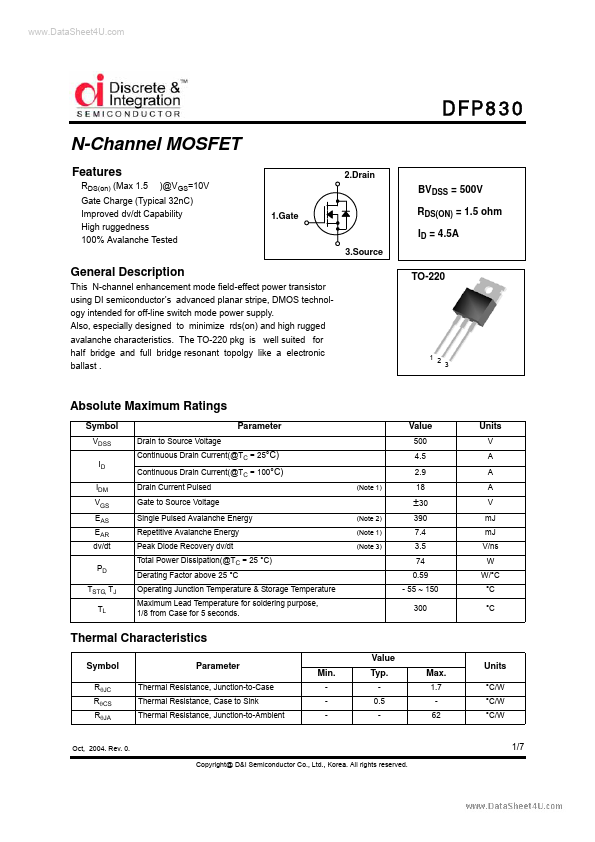
RDS(on) (Max 1.5 )@VGS=10V 1.Gate 2.Drain Gate Charge (Typical 32nC) Improved dv/dt Capability High ruggedness 100% Avalanche Tested BVDSS = 500V RDS(ON) = 1.5 ohm ID = 4.5A 3.Source GENERAL DESCRIPTION
Also, especially designed to minimize rds(on) and high rugged avalanche characteristics. TO-220 1 2 3 ABSOLUTE MAXIMUM RATINGS
Symbol VDSS ID IDM VGS EAS EAR dv/dt PD TSTG, TJ TL Drain to Source Voltage Continuous Drain Current(@TC = 25°C) Continuous Drain Current(@TC = 100°C) Drain Current Pulsed Gate to Source Voltage Single Pulsed Avalanche Energy Repetitive Avalanche Energy Peak Diode Recovery dv/dt Total Power Dissipation(@TC = 25 °C) Derating Factor above 25 °C Operating Junction Temperature & Storage Temperature Maximum Lead Temperature for soldering purpose, 1/8 from Case for 5 seconds. (Note 2) (Note 1) (Note 3) (Note 1) Parameter Value 500 4.5 2.9 18 Units V A A A V mJ mJ V/ns W W/°C °C °C ±30 390 7.4 3.5 74 0.59 - 55 ~ 150 300 Thermal Characteristics Symbol RθJC RθCS RθJA Parameter Thermal Resistance, Junction-to-Case Thermal Resistance, Case to Sink Thermal Resistance, Junction-to-Ambient Value Min. - Typ. DnI