F50D1G41LB-66YG2ME
F50D1G41LB-66YG2ME is 1.8V 1 Gbit SPI-NAND Flash Memory manufactured by Elite Semiconductor Microelectronics Technology.
- Part of the F50D1G41LB-50YG2M comparator family.
- Part of the F50D1G41LB-50YG2M comparator family.
ESMT
Flash
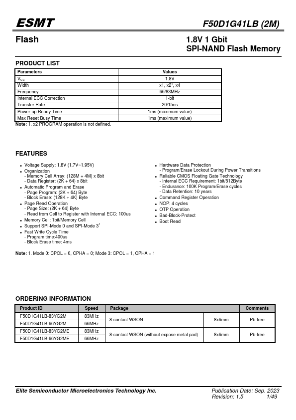
PRODUCT LIST
Parameters VCC Width Frequency Internal ECC Correction Transfer Rate Power-up Ready Time Max Reset Busy Time Note: 1. x2 PROGRAM operation is not defined.
F50D1G41LB (2M)
1.8V 1 Gbit SPI-NAND Flash Memory
Values 1.8V x1, x21, x4 66/83MHz
1-bit 20/15ns 1ms (maximum value) 1ms (maximum value)
Features
- Voltage Supply: 1.8V (1.7V~1.95V)
- Organization
- Memory Cell Array: (128M + 4M) x 8bit
- Data Register: (2K + 64) x 8bit
- Automatic Program and Erase
- Page Program: (2K + 64) Byte
- Block Erase: (128K + 4K) Byte
- Page Read Operation
- Page Size: (2K + 64) Byte
- Read from Cell to Register with Internal ECC: 100us
- Memory Cell: 1bit/Memory Cell
- Support...