F50L1G41LC
Description
Serial peripheral interface (SPI) NAND is an SLC NAND Flash memory device that provides a cost-effective nonvolatile memory storage solution where pin count must be kept to a minimum. It is also an alternative solution to SPI NOR, offering superior writes performance and cost per bit over SPI NOR.
Key Features
- Voltage Supply: 3.3V (2.7V~3.6V)
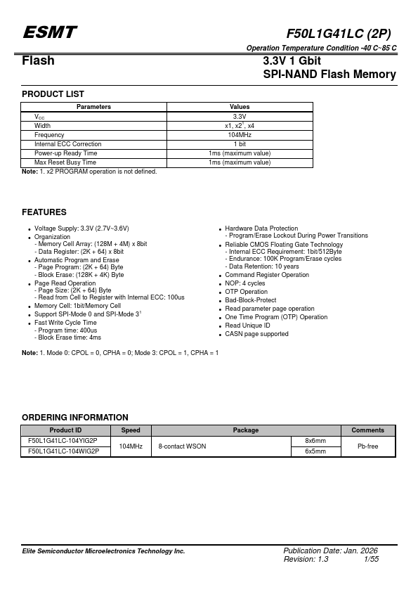
- Organization - Memory Cell Array: (128M + 4M) x 8bit - Data Register: (2K + 64) x 8bit
- Automatic Program and Erase - Page Program: (2K + 64) Byte - Block Erase: (128K + 4K) Byte
- Page Read Operation - Page Size: (2K + 64) Byte - Read from Cell to Register with Internal ECC: 100us
- Memory Cell: 1bit/Memory Cell
- Support SPI-Mode 0 and SPI-Mode 31
- Fast Write Cycle Time - Program time: 400us - Block Erase time: 4ms
- Hardware Data Protection - Program/Erase Lockout During Power Transitions
- Reliable CMOS Floating Gate Technology - Internal ECC Requirement: 1bit/512Byte - Endurance: 100K Program/Erase cycles - Data Retention: 10 years
- Command Register Operation