EIA1114-2
EIA1114-2 is 11.0-14.0 GHz 2-Watt Internally Matched Power FET manufactured by Excelics Semiconductor.
FEATURES
- -
- -
- -
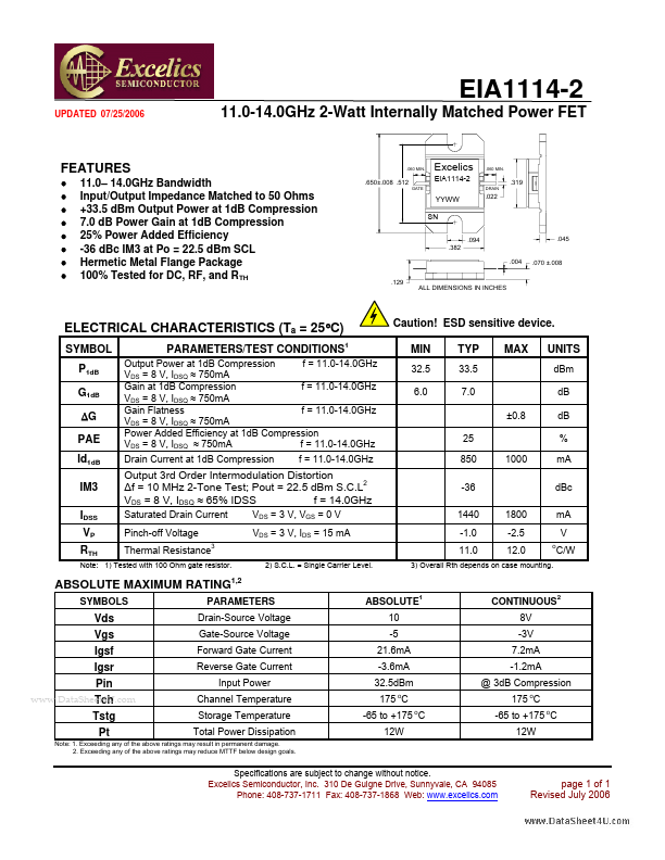
- - 11.0- 14.0GHz Bandwidth Input/Output Impedance Matched to 50 Ohms +33.5 d Bm Output Power at 1d B pression 7.0 d B Power Gain at 1d B pression 25% Power Added Efficiency -36 d Bc IM3 at Po = 22.5 d Bm SCL Hermetic Metal Flange Package 100% Tested for DC, RF, and RTH
.060 MIN.
Excelics
YYWW SN
.094 .382
.060 MIN.
.650±.008 .512
GATE
.319
DRAIN
.022
.045 .004
.070 ±.008
.129
ALL DIMENSIONS IN INCHES
ELECTRICAL CHARACTERISTICS (Ta = 25°C)
SYMBOL P1d B G1d B ∆G PAE Id1d B IM3 IDSS VP RTH PARAMETERS/TEST CONDITIONS1
Output Power at 1d B pression f = 11.0-14.0GHz VDS = 8 V, IDSQ ≈ 750m A Gain at 1d B pression f = 11.0-14.0GHz VDS = 8 V, IDSQ ≈ 750m A Gain Flatness f = 11.0-14.0GHz VDS = 8 V, IDSQ ≈ 750m A Power Added Efficiency at 1d B pression f = 11.0-14.0GHz VDS = 8 V, IDSQ ≈ 750m A Drain Current at 1d B pression f = 11.0-14.0GHz
Caution! ESD sensitive device. MIN
32.5 6.0
33.5 7.0
UNITS d Bm d B
±0.8 25 850 -36 1440 -1.0 11.0 1800 -2.5 12.0 o d B %
1000 m A d Bc m A V C/W
Output 3rd Order Intermodulation Distortion ∆f = 10 MHz 2-Tone Test; Pout = 22.5 d Bm S.C.L2 VDS = 8 V, IDSQ ≈ 65% IDSS f = 14.0GHz
Saturated Drain Current Pinch-off Voltage Thermal Resistance
VDS = 3 V, VGS = 0 V VDS = 3 V, IDS = 15 m A
2) S.C.L. = Single Carrier Level.
Note: 1) Tested with 100 Ohm gate resistor.
3) Overall Rth depends on case mounting.
ABSOLUTE MAXIMUM RATING1,2
SYMBOLS PARAMETERS Drain-Source Voltage Gate-Source Voltage Forward Gate Current Reverse Gate Current Input Power Channel Temperature Storage Temperature Total Power Dissipation ABSOLUTE1 10 -5 21.6m A -3.6m A 32.5d Bm o 175 C o -65 to +175 C
CONTINUOUS2 8V -3V 7.2m A -1.2m A @ 3d B pression 175 o C -65 to +175 o C...