Excelliance MOS EMBA3P03JS
P-Channel Logic Level Enhancement Mode Field Effect Transistor
| Part No. | EMBA3P03JS |
|---|---|
| Datasheet | EMBA3P03JS Download |
| Manufacturer |  Excelliance MOS |
| Description | P-Channel Logic Level Enhancement Mode Field Effect Transistor |
| Buy | Stock & Price |
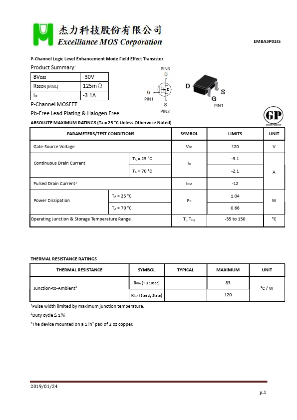
ABSOLUTE MAXIMUM RATINGS
(TA = 25 °C Unless Otherwise Noted) PARAMETERS/TEST CONDITIONS SYMBOL Gate-Source Voltage VGS Continuous Drain Current Pulsed Drain Current1 TA = 25 °C ID TA = 70 °C IDM Power Dissipation TA = 25 °C TA = 70 °C Operating Junction & Storage Temperature Range PD Tj, Tstg EMBA3P03JS LIMITS ±20 -3.1 -2.1 -12 1.04 0.66 -55 to 150 UNIT V A W °C THERMAL RESISTANCE RATINGS THERMAL RESISTANCE SYMBOL Junction-to-Ambient3 R●JA (T ≤ 10sec) R●JA (Steady State) 1Pulse width limited by maximum junction temperature. 2Duty cycle 1% 3The device mounted on a 1 in2 pad of 2 oz copper. TYPICAL MAXIMUM 83 120 UNIT °C / W 2019/01/24 p.1 EMBA3P03JSELECTRICAL CHARACTERISTICS
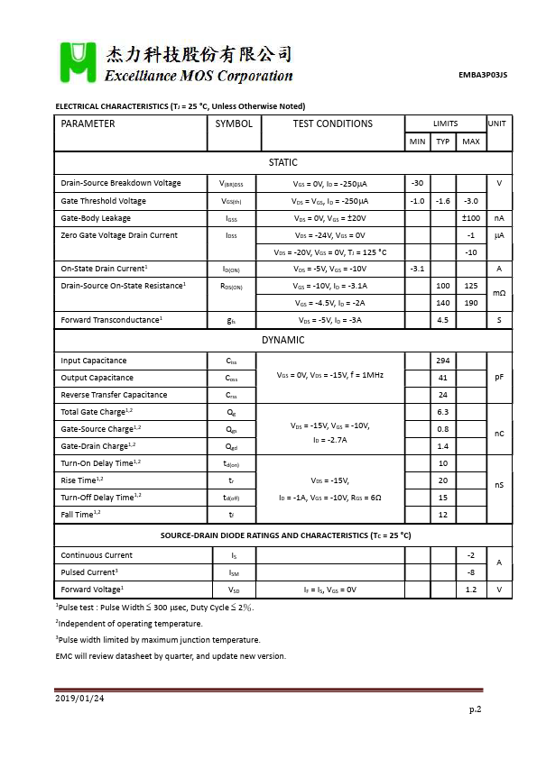
(TJ = 25 °C, Unless Otherwise Noted) PARAMETER SYMBOL TEST CONDITIONS LIMITS UNIT MIN TYP MAX STATIC Drain-Source Breakdown Voltage Gate Threshold Voltage Gate-Body Leakage Zero Gate Voltage Drain Current On-State Drain Current1 Drain-Source On-State Resistance1 Forward Transconductance1 Input Capacitance Output...