EMBA5P06J
EMBA5P06J is P-Channel Logic Level Enhancement Mode Field Effect Transistor manufactured by Excelliance MOS.
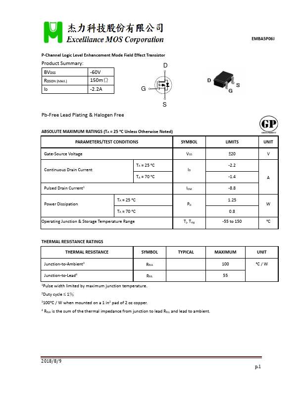
P-Channel Logic Level Enhancement Mode Field Effect Transistor
Product Summary:
BVDSS
-60V
RDSON (MAX.)
150mΩ
-2.2A
S Pb-Free Lead Plating & Halogen Free
ABSOLUTE MAXIMUM RATINGS (TA = 25 °C Unless Otherwise Noted) PARAMETERS/TEST CONDITIONS
SYMBOL
Gate-Source Voltage
Continuous Drain Current Pulsed Drain Current1
TA = 25 °C ID
TA = 70 °C
Power Dissipation
TA = 25 °C TA = 70 °C
Operating Junction & Storage Temperature Range
PD Tj, Tstg
LIMITS ±20 -2.2 -1.4 -8.8 1.25 0.8
-55 to 150
UNIT V
W °C
THERMAL RESISTANCE RATINGS THERMAL RESISTANCE
SYMBOL
TYPICAL
MAXIMUM
Junction-to-Ambient3
RθJA
Junction-to-Lead4
RθJL
1Pulse width limited by maximum junction temperature. 2Duty cycle ≤ 1% 3100°C / W when mounted on a 1 in2 pad of 2 oz copper. 4 RθJA is the sum of the thermal impedance from junction to lead RθJL and lead to ambient.
UNIT °C /...