EMF30N02JS
EMF30N02JS is N-Channel Logic Level Enhancement Mode Field Effect Transistor manufactured by Excelliance MOS.
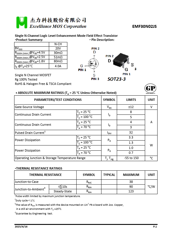
Description
:
N-CH
BVDSS RDSON (MAX.)@VGS=4.5V RDSON (MAX.)@VGS=2.5V RDSON (MAX.)@VGS=1.8V
20V 30mΩ 51mΩ 80mΩ
ID @TA=25℃
4.0A
Single N Channel MOSFET Rg 100% Tested Ro HS & Halogen Free & TSCA pliant
- ABSOLUTE MAXIMUM RATINGS (TA = 25 °C Unless Otherwise Noted)
PARAMETERS/TEST CONDITIONS
SYMBOL
Gate-Source Voltage
Continuous Drain Current
Continuous Drain Current Pulsed Drain Current1
TC = 25 °C TC = 100 °C TA = 25 °C TA = 70 °C
Power Dissipation
TC = 25 °C TC = 100 °C
Power Dissipation
TA = 25 °C TA = 70 °C
Operating Junction & Storage Temperature Range
VGS ID
ID IDM PD
PD Tj, Tstg
LIMITS
±12 8 5 4 3 32 3.3 1.3 1.0 0.7 -55 to 150
UNIT V A
W °C
- THERMAL RESISTANCE RATINGS
THERMAL RESISTANCE
SYMBOL TYPICAL MAXIMUM
Junction-to-Case
RθJC
Junction-to-Ambient3 t≦10s Steady-State
RθJA RθJA
90 123
1Pulse width limited by maximum junction temperature.
2Duty cycle < 1%
3The value of RθJA is measured with the device mounted on 1in2 FR-4 board with 2oz. Copper, in a still air environment with TA =25°C.
4Guarantee by Engineering...