FNK FNK3316
N-Channel MOSFET
| Part No. | FNK3316 |
|---|---|
| Datasheet | FNK3316 Download |
| Manufacturer |  FNK |
| Description | N-Channel MOSFET |
| Buy | Stock & Price |
GENERAL DESCRIPTION
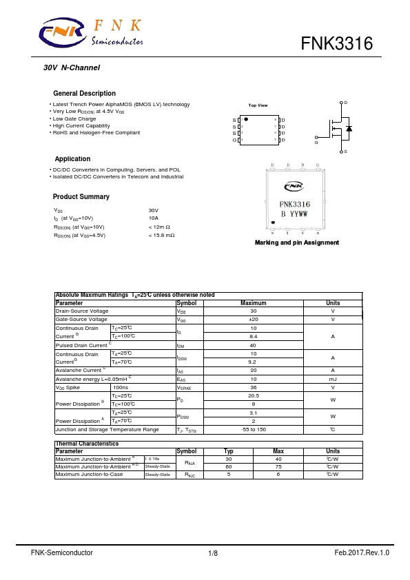
● Latest Trench Power AlphaMOS (αMOS LV) technology● Very Low RDS(ON) at 4.5V VGS
● Low Gate Charge
● High Current Capability
● RoHS and Halogen-Free Compliant Application
● DC/DC Converters in Computing, Servers, and POL
● Isolated DC/DC Converters in Telecom and Industrial Product Summary VDS ID (at VGS=10V) RDS(ON) (at VGS=10V) RDS(ON) (at VGS=4.5V) 30V 10A < 12m Ω < 15.8 mΩ FNK3316 Top View 18 27 36 45 D G S V2#W$(3ÿ2(Uÿ%$(ÿQ!!$3(T4(&ÿ
ABSOLUTE MAXIMUM RATINGS
TA=25°C unless otherwise noted Parameter Symbol Drain-Source Voltage VDS Gate-Source Voltage VGS Continuous Drain TC=25°C Current G TC=100°C Pulsed Drain Current C ID IDM Continuous Drain CurrentG TA=25°C TA=70°C Avalanche Current C Avalanche energy L=0.05mH C IDSM IAS EAS VDS Spike 100ns VSPIKE TC=25°C Power Dissipation B TC=100°C PD TA=25°C Power Dissipation A TA=70°C PDSM Junction and Storage Temperature Range TJ, TSTG Maxi