FNK4620
FNK4620 is Complementary Enhancement Mode Field Effect Transistor manufactured by FNK.
Description
The FNK4620 uses advanced trench technology MOSFETs to provide excellent RDS(ON) and low gate charge. The plementary MOSFETs may be used in inverter and other applications.
Features n-channel
VDS (V) = 30V ID = 7.2A (VGS=10V) RDS(ON) < 21mΩ (VGS=10V) < 27mΩ (VGS=4.5V) p-channel
-30V
-5.3A (VGS = -10V) RDS(ON)
< 30mΩ (VGS = -10V) < 44mΩ (VGS = -4.5V)
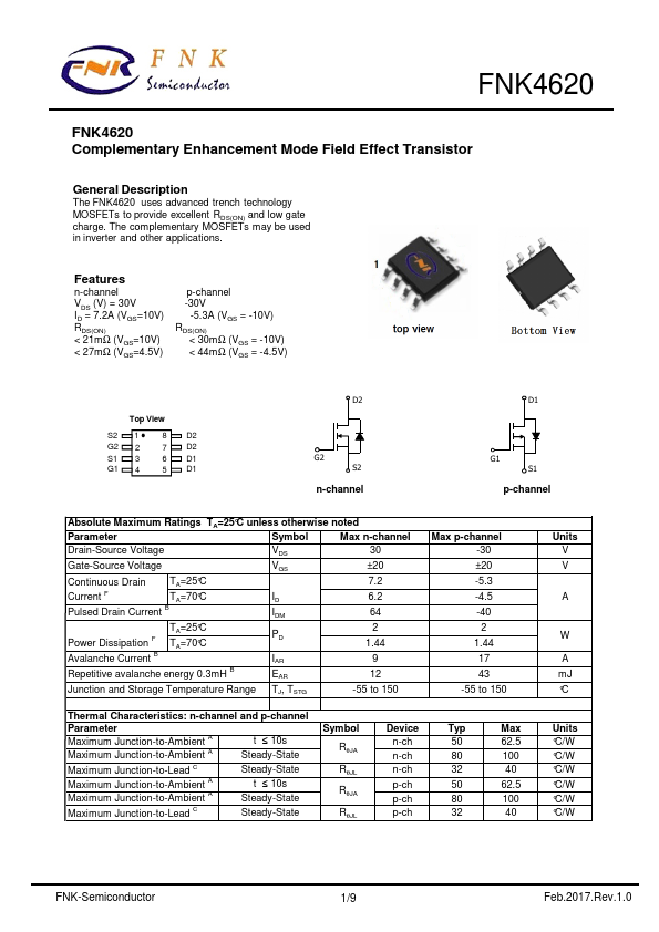
Top View
S2 1 G2 2 S1 3 G1 4
7 6 5
D2 D2 D1 D1
D2
G2 S2 n-channel
D1
G1 S1 p-channel
Absolute Maximum Ratings TA=25°C unless otherwise noted
Parameter
Symbol
Max n-channel
Drain-Source Voltage
VDS 30
Gate-Source Voltage
VGS ±20
Continuous Drain TA=25°C
Current F
TA=70°C
Pulsed Drain Current B
ID IDM
7.2 6.2 64
Power Dissipation F Avalanche Current B
TA=25°C TA=70°C
Repetitive avalanche energy 0.3m H B
IAR EAR
2 1.44
9 12
Junction and Storage Temperature Range TJ, TSTG
-55 to 150
Max p-channel -30...