FDD850N10L Overview
Key Specifications
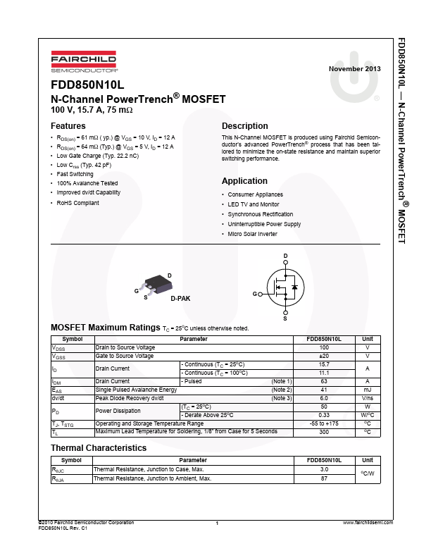
Package: DPAK
Mount Type: Surface Mount
Pins: 3
Height: 2.39 mm
Description
This N-Channel MOSFET is produced using Fairchld Semiconductor’s advanced PowerTrench® process that has been tailored to minimize the on-state resistance and maintain superior switching performance.
Key Features
- RDS(on) = 61 mΩ ( yp.) @ VGS = 10 V, ID = 12 A
- RDS(on) = 64 mΩ (Typ.) @ VGS = 5 V, ID = 12 A
- Low Gate Charge (Typ. 22.2 nC)
- Low Crss (Typ. 42 pF)
- Fast Switching
- 100% Avalanche Tested
- Improved dv/dt Capability
- RoHS Compliant