FDFMA2P029Z
FDFMA2P029Z is Integrated P-Channel PowerTrench MOSFET and Schottky Diode manufactured by Fairchild Semiconductor.
FDFMA2P029Z Integrated P-Channel Power Trench® MOSFET and Schottky Diode
December 2006
- 20V,
- 3.1A, 95mΩ Features
MOSFET
Integrated P-Channel Power Trench® MOSFET and Schottky Diode
General Description
This device is designed specifically as a single package solution for the battery charge switch in cellular handset and other ultraportable applications. It Features a MOSFET with very low onstate resistance and an independently connected low forward voltage schottky diode allows for minimum conduction losses. The Micro FET 2X2 package offers exceptional thermal performance for its physical size and is well suited to linear mode applications.
- Max r DS(on) = 95mΩ at VGS =
- 4.5V, ID =
- 3.1A
- Max r DS(on) = 141mΩ at VGS =
- 2.5V, ID =
- 2.5A
Schottky
- VF < 0.37V @ 500m A
- Low profile
- 0.8 mm maximum
- in the new package Micro FET 2x2 mm
- Ro HS pliant
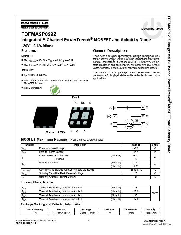
Pin 1 A NC D A 1 NC 2 D 3 Micro FET 2X2 C G S 6 C 5 G 4 S
..
MOSFET Maximum Ratings TA = 25°C unless otherwise noted
Symbol VDS VGS ID PD TJ, TSTG VRRM IO Parameter Drain to Source Voltage Gate to Source Voltage Drain Current -Continuous -Pulsed Power Dissipation Operating and Storage Junction Temperature Range Schottky Repetitive Peak Reverse Voltage Schottky Average Forward Current (Note 1a) (Note 1b) (Note 1a) Ratings
- 20 ±12
- 3.1 -6 1.4 0.7
- 55 to +150 20 2 Units V V A W °C V A
Thermal Characteristics
RθJA RθJA RθJA RθJA Thermal Resistance, Junction to Ambient Thermal Resistance, Junction to Ambient Thermal Resistance, Junction to Ambient Thermal Resistance, Junction to Ambient (Note 1a) (Note 1b) (Note 1c) (Note 1d) 86 173 86 140 °C/W
Package Marking and Ordering...